verilog hdl lrm - extra materials
TRANSCRIPT
OVI Verilog HDL LRM
Version 1.0
Contents
Introduction 1 Cover Pages/Copyrights ............................................................................................................1 1.0 Overview .............................................................................................................................2 1.1 Criteria for Selecting Material for This Manual ..................................................................3 1.2 The Contents of the Reference Manual................................................................................4
Lexical Conventions 6 2.0 Lexical Conventions Overview............................................................................................6 2.1 Operators .............................................................................................................................6 2.2 White Space and Comments ................................................................................................6 2.3 Numbers...............................................................................................................................7 2.4 Strings..................................................................................................................................9
2.4.1 String Variable Declaration ................................................................................9 2.4.2 String Manipulation............................................................................................9 2.4.3 Special Characters in Strings............................................................................10
2.5 Identifiers, Keywords, and System Names ........................................................................10 2.5.1 Escaped Identifiers ...........................................................................................11 2.5.2 Keywords..........................................................................................................12 2.5.3 The $keyword Construct ..................................................................................12 2.5.4 The `keyword Construct ...................................................................................12
2.6 Text Substitutions ..............................................................................................................13
Data Types 15 3.0 Data Types Overview ........................................................................................................ 15 3.1 Value Set............................................................................................................................15 3.2 Registers and Nets .............................................................................................................15
3.2.1 Nets...................................................................................................................15 3.2.2 Registers ...........................................................................................................16 3.2.3 Declaration Syntax ...........................................................................................16 3.2.4 Declaration Examples.......................................................................................18
3.3 Vectors...............................................................................................................................18 3.3.1 Specifying Vectors ...........................................................................................18 3.3.2 Vector Net Accessibility...................................................................................19
3.4 Strengths ............................................................................................................................19 3.4.1 Charge Strength ................................................................................................19 3.4.2 Drive Strength ..................................................................................................20
3.5 Implicit Declarations..........................................................................................................20 3.6 Net Initialization ................................................................................................................20 3.7 Net Types...........................................................................................................................20
3.7.1 wire and tri Nets ...............................................................................................20 3.7.2 Wired Nets........................................................................................................21 3.7.3 trireg Net...........................................................................................................22 3.7.4 tri0 and tri1 Nets...............................................................................................25
Verilog HDL LRM Contents • i
3.7.5 supply Nets .......................................................................................................25 3.8 Memories ...........................................................................................................................25 3.9 Integers and Times.............................................................................................................26 3.10 Real Numbers ..................................................................................................................27
3.10.1 Declaration Syntax for Real Numbers ............................................................28 3.10.2 Specifying Real Numbers...............................................................................28 3.10.3 Operators and Real Numbers..........................................................................28 3.10.4 Conversion......................................................................................................29
3.11 Parameters........................................................................................................................29
Expressions 31 4.0 Expressions Overview .......................................................................................................31 4.1 Operators ...........................................................................................................................31
4.1.1 Binary Operator Precedence.............................................................................33 4.1.2 Numeric Conventions in Expressions...............................................................34 4.1.3 Arithmetic Operators ........................................................................................34 4.1.4 Arithmetic Expressions with Registers and Integers ........................................35 4.1.5 Relational Operators .........................................................................................36 4.1.6 Equality Operators............................................................................................36 4.1.7 Logical Operators .............................................................................................37 4.1.8 Bit-Wise Operators ...........................................................................................38 4.1.9 Reduction Operators .........................................................................................39 4.1.10 Syntax Restrictions.........................................................................................40 4.1.11 Shift Operators................................................................................................41 4.1.12 Conditional Operator ......................................................................................41 4.1.13 Concatenations ...............................................................................................42
4.2 Operands............................................................................................................................43 4.2.1 Net and Register Bit Addressing ......................................................................43 4.2.2 Memory Addressing .........................................................................................44 4.2.3 Strings...............................................................................................................45 4.2.4 String Operations..............................................................................................46 4.2.5 String Value Padding and Potential Problems..................................................46 4.2.6 Null String Handling ........................................................................................47
4.3 Minimum, Typical, Maximum Delay Expressions ............................................................47 4.4 Expression Bit Lengths......................................................................................................48
4.4.1 An Example of an Expression Bit Length Problem..........................................48 4.4.2 Verilog Rules for Expression Bit Lengths........................................................49
Assignments 51 5.0 Assignments Overview......................................................................................................51 5.1 Continuous Assignments ...................................................................................................51
5.1.1 The Net Declaration Assignment......................................................................52 5.1.2 The Continuous Assignment Statement............................................................53 5.1.3 Delays...............................................................................................................54 5.1.4 Strength ............................................................................................................55
5.2 Procedural Assignments ....................................................................................................56
Gate and Switch Level Modeling 57 6.0 Gate and Switch Level Modeling Overview......................................................................57 6.1 Gate and Switch Declaration Syntax .................................................................................57 6.2 and, nand, nor, or, xor, and xnor Gates..............................................................................60 6.3 buf and not Gates ...............................................................................................................61 6.4 bufif1, bufif0, notif1, and notif0 Gates ..............................................................................62 6.5 MOS Switches ...................................................................................................................63
Verilog HDL LRM Contents • ii
6.6 Bidirectional Pass Switches ...............................................................................................65 6.7 cmos Gates.........................................................................................................................66 6.8 pullup and pulldown Sources.............................................................................................66 6.9 Implicit Net Declarations...................................................................................................67 6.10 Logic Strength Modeling .................................................................................................67 6.11 Strengths and Values of Combined Signals .....................................................................69
6.11.1 Combined Signals of Unambiguous Strength.................................................69 6.11.2 Ambiguous Strengths: Sources and Combinations.........................................70 6.11.3 Ambiguous Strength Signals and Unambiguous Signals................................75 6.11.4 Wired Logic Net Types ..................................................................................78
6.12 Strength Reduction by Non-Resistive Devices ................................................................80 6.13 Strength Reduction by Resistive Devices ........................................................................80 6.14 Strengths of Net Types .................................................................................................... 80
6.14.1 tri1 Net Strengths............................................................................................80 6.14.2 trireg Strength.................................................................................................80 6.14.3 supply0 and supply1 Net Strengths ................................................................81
6.15 Gate and Net Delays ........................................................................................................81 6.15.1 min/typ/max Delays........................................................................................83 6.15.2 trireg Net Charge Decay .................................................................................83
User-Defined Primitives (UDPs) 86 7.0 UDP Overview...................................................................................................................86 7.1 Syntax ................................................................................................................................86 7.2 UDP Definition..................................................................................................................88
7.2.1 UDP Terminals.................................................................................................88 7.2.2 UDP Declarations.............................................................................................89 7.2.3 Sequential UDP initial Statement .....................................................................89 7.2.4 UDP State Table ...............................................................................................89
7.3 Combinational UDPs ......................................................................................................... 90 7.4 Level-Sensitive Sequential UDPs ......................................................................................91 7.5 Edge-Sensitive UDPs.........................................................................................................92 7.6 Sequential UDP Initialization ............................................................................................93 7.7 UDP Instances ...................................................................................................................95 7.8 Symbols to Enhance Readability .......................................................................................96 7.9 Mixing Level and Edge-Sensitive Descriptions.................................................................97 7.10 Reducing Pessimism........................................................................................................98 7.11 Level-Sensitive Dominance .............................................................................................99 7.12 Summary of Symbols.....................................................................................................100 7.13 Examples .......................................................................................................................101
Behavioral Modeling 103 8.1 Behavioral Model Overview............................................................................................103 8.2 Procedural Assignments ..................................................................................................104
8.2.1 Blocking Procedural Assignments..................................................................105 8.2.2 The Non-Blocking Procedural Assignment....................................................106 8.2.3 How the Simulator Processes Blocking and Non-Blocking Procedural Assignments ............................................................................................................110
8.3 Conditional Statement......................................................................................................110 8.3.1 if-else-if Construct..........................................................................................112 8.3.2 Example..........................................................................................................113
8.4 Case Statement.................................................................................................................114 8.4.1 Case Statement with Don’t-Cares...................................................................116
8.5 Looping Statements .........................................................................................................117 8.5.1 forever Loop ...................................................................................................118
Verilog HDL LRM Contents • iii
8.5.2 repeat Loop Example......................................................................................119 8.5.3 while Loop Example.......................................................................................119 8.5.4 for Loop Examples .........................................................................................120
8.6 Procedural Timing Controls.............................................................................................121 8.6.1 Delay Control .................................................................................................122 8.6.2 Event Control .................................................................................................122 8.6.3 Named Events.................................................................................................123 8.6.4 Event OR Construct........................................................................................124 8.6.5 Level-Sensitive Event Control........................................................................124 8.6.6 Intra-Assignment Timing Controls.................................................................125
8.7 Block Statements .............................................................................................................128 8.7.1 Sequential Blocks ...........................................................................................128 8.7.2 Parallel Blocks................................................................................................130 8.7.3 Block Names ..................................................................................................131 8.7.4 Start and Finish Times....................................................................................131
8.8 Structured Procedures ...................................................................................................... 133 8.8.1 initial Statement..............................................................................................133 8.8.2 always Statement ............................................................................................134 8.8.3 Examples ........................................................................................................135
Tasks and Functions 138 9.0 Tasks and Functions Overview........................................................................................138 9.1 Distinctions between Tasks and Functions ......................................................................138 9.2 Tasks and Task Enabling .................................................................................................138
9.2.1 Defining a Task ..............................................................................................139 9.2.2 Task Enabling and Argument Passing............................................................140 9.2.3 Task Example .................................................................................................141 9.2.4 Effect of Enabling an Already Active Task....................................................142
9.3 Functions and Function Calling .......................................................................................142 9.3.1 Defining a Function........................................................................................143 9.3.2 Returning a Value from a Function ................................................................144 9.3.3 Calling a Function ..........................................................................................144 9.3.4 Function Rules................................................................................................144 9.3.5 Function Example...........................................................................................145
Disabling of Named Blocks and Tasks 146 10.0 Disabling Blocks and Tasks Overview ..........................................................................146
Procedural Continuous Assignments 151 11.0 Procedural Continuous Assignment Overview ..............................................................151 11.1 The assign and deassign Procedural Statements ............................................................151 11.2 The force and release Procedural Statements.................................................................152
Hierarchical Structures 154 12.0 Hierarchical Structures Overview..................................................................................154 12.1 Modules .........................................................................................................................154
12.1.1 Top-Level Modules ......................................................................................155 12.1.2 Module Instantiation.....................................................................................155 12.1.3 Module Definition and Instance Example ....................................................156
12.2 Overriding Module Parameter Values ...........................................................................158 12.2.1 defparam Statement ......................................................................................158 12.2.2 Module Instance Parameter Value Assignment............................................159 12.2.3 Parameter Dependence .................................................................................160
Verilog HDL LRM Contents • iv
12.3 Macro Modules..............................................................................................................160 12.3.1 Specifying Macro Modules ..........................................................................161 12.3.2 Instances of Macro Modules.........................................................................161
12.4 Ports ...............................................................................................................................161 12.4.1 Port Definition ..............................................................................................161 12.4.2 Port Declarations ..........................................................................................162 12.4.3 Connecting Module Ports by Ordered List ...................................................162 12.4.4 Connecting Module Ports by Name..............................................................163 12.4.5 Real Numbers in Port Connections...............................................................165 12.4.6 Port Collapsing .............................................................................................165 12.4.7 Port Connection Rules ..................................................................................165
12.5 Hierarchical Names........................................................................................................167 12.5.1 Upwards Name Referencing.........................................................................170
12.6 Scope Rules ...................................................................................................................172
Specify Blocks 174 13.0 Specify Blocks Overview ..............................................................................................174 13.1 Declaring Parameters in Specify Blocks........................................................................175 13.2 Module Path Delays.......................................................................................................176
13.2.0 Module Path Delay Overview ......................................................................176 13.2.1 Describing Module Paths..............................................................................179 13.2.2 Declaring Multiple Module Paths in a Single Statement..............................182 13.2.3 Assigning Delays to Module Paths...............................................................183 13.2.4 Specifying Transition Delays on Module Paths ...........................................184 13.2.5 Handling X Transitions ................................................................................186 13.2.6 State Dependent Path Delays (SDPDs) ........................................................187 13.2.7 Driving Wired Logic ....................................................................................192 13.2.8 Module Path Polarity ....................................................................................193 13.2.9 Qualified Paths .............................................................................................195
Formal Syntax Definition 201 A.0 Syntax Overview.............................................................................................................201 A.1 Source Text .....................................................................................................................201 A.2 Declarations ....................................................................................................................204 A.3 Primitive instances ..........................................................................................................206 A.4 Module Instantiations...................................................................................................... 207 A.5 Behavioral Statements ....................................................................................................208 A.6 Specify Section ...............................................................................................................210 A.7 Expressions .....................................................................................................................213 A.8 General............................................................................................................................215
System Tasks and Functions 216 B.0 System Tasks Overview..................................................................................................216 B.1 The Display and Write Tasks ..........................................................................................216
B.1.1 Escape Sequences for Special Characters ......................................................217 B.1.2 Format Specifications ....................................................................................218 B.1.3 Size of Displayed Data...................................................................................219 B.1.4 Unknown and High Impedance Values..........................................................220 B.1.5 Strength Format .............................................................................................221 B.1.6 Hierarchical Name Format.............................................................................223 B.1.7 String Format .................................................................................................223
B.2 Strobed Monitoring .........................................................................................................223 B.3 Continuous Monitoring ...................................................................................................224 B.4 Timescale System Functions...........................................................................................225
Verilog HDL LRM Contents • v
B.4.1 The $time System Function ...........................................................................225 B.4.2 The $realtime System Function .....................................................................226 B.4.3 The %t Format Specification .........................................................................227
B.5 Timescale System Tasks .................................................................................................227 B.5.1 The $printtimescale System Task ..................................................................227 B.5.2 The $timeformat System Task .......................................................................228
B.6 Simulation Time—The $time Function ..........................................................................231 B.7 Finish System Task .........................................................................................................231 B.8 Functions and Tasks for Reals ........................................................................................231 B.9 Timing Checks ................................................................................................................232
B.9.1 The $setup Timing Check..............................................................................233 B.9.2 The $hold Timing Check ...............................................................................234 B.9.3 The $width Timing Check .............................................................................234 B.9.4 The $period Timing Check ............................................................................236 B.9.5 The $skew Timing Check ..............................................................................236 B.9.6 The $recovery Timing Check ........................................................................237 B.9.7 The $setuphold Timing Check.......................................................................238 B.9.8 Edge-Control Specifiers.................................................................................239 B.9.9 Notifiers: User-Defined Responses to Timing Violations .............................240 B.9.10 Enabling Timing Checks with Conditioned Events .....................................242
Compiler Directives 245 C.0 Compiler Overview.........................................................................................................245 C.1 `define .............................................................................................................................245 C.2 `default_nettype ..............................................................................................................246 C.3 `unconnected_drive and `nounconnected_drive..............................................................247 C.4 `resetall............................................................................................................................247 C.5 `timescale ........................................................................................................................247
List of System Task and System Function Keywords 250 D.0 System Tasks Overview..................................................................................................250 D.1 $bitstoreal .......................................................................................................................251 D.2 $countdrivers ..................................................................................................................251 D.3 $display...........................................................................................................................253 D.4 Value Change Dump File Tasks .....................................................................................253 D.5 File Output ......................................................................................................................253 D.6 $finish .............................................................................................................................255 D.7 $getpattern ......................................................................................................................255 D.8 $history ..........................................................................................................................257 D.9 $incsave .........................................................................................................................257 D.10 $input ...........................................................................................................................257 D.11 $itor...............................................................................................................................257 D.12 $key and $nokey .......................................................................................................... 257 D.13 $list ...............................................................................................................................258 D.14 $log and $nolog ...........................................................................................................258 D.15 $monitor, $monitoron, $monitoroff ..............................................................................258 D.16 $printtimescale..............................................................................................................258 D.17 $readmemb and $readmemh .........................................................................................258 D.18 $realtime .......................................................................................................................260 D.19 $realtobits......................................................................................................................260 D.20 $reset, $reset_count and $reset_value...........................................................................260 D.21 $restart ..........................................................................................................................262 D.22 $rtoi...............................................................................................................................262 D.23 Saving and Restarting ...................................................................................................262
Verilog HDL LRM Contents • vi
D.23.1 Incremental Save and Restart ......................................................................262 D.24 $scale ............................................................................................................................263 D.25 $scope ...........................................................................................................................263 D.26 $showscopes .................................................................................................................264 D.27 $showvars .....................................................................................................................264 D.28 $sreadmemb and $sreadmemh ......................................................................................264 D.29 $stime............................................................................................................................265 D.30 $stop..............................................................................................................................265 D.31 $strobe...........................................................................................................................265 D.32 $time, $stime and $realtime ..........................................................................................265 D.33 $timeformat...................................................................................................................265 D.34 $write ............................................................................................................................265
List of Compiler Directive Keywords 266 E.0 Compilier Directive Overview ........................................................................................266 E.1 `accelerate and `noaccelerate...........................................................................................267 E.2 `autoexpand_vectornets...................................................................................................267 E.3 `celldefine and `endcelldefine .........................................................................................267 E.4 `default_nettype...............................................................................................................267 E.5 `define .............................................................................................................................267 E.6 `expand_vectornets..........................................................................................................267 E.7 `ifdef, `else, `endif ...........................................................................................................267
E.7.1 Nesting the `ifdef, `else, and `endif Compiler Directives ..............................269 E.7.2 Defining Variable Names to Control Conditional Compilation.....................270
E.8 `include............................................................................................................................270 E.9 `noexpand_vectornets......................................................................................................271 E.10 `protect and `endprotect.................................................................................................271 E.11 `protected and `endprotected .........................................................................................271 E.12 `remove_gatenames and `noremove_gatenames ...........................................................271 E.13 `remove_netnames and `noremove_netnames...............................................................272 E.14 `resetall ..........................................................................................................................272 E.15 `timescale ......................................................................................................................272 E.16 `unconnected_drive and `nounconnected_drive ............................................................272
List of Keywords 273 Keywords...............................................................................................................................273
Index 276
Verilog HDL LRM Contents • vii
Introduction
Cover Pages/Copyrights
Verilog Hardware Description
Language Reference Manual
(LRM)
Version 1.0
November, 1991
Open Verilog International
Notice: This manual has been superceded by the IEEE 1364 specification for the Verilog Hardware Description Language, which can only be purchased from IEEE.
Copyright© 1991 by Open Verilog International (OVI), Inc. All rights reserved.
Copyright© 1995 for the electronic Help version of the OVI LRM 1.0 by Simucad, Inc. All rights reserved.
No part of this work covered by the copyright hereon may be reproduced or used in any form or by any means --- graphic, electronic, or mechanical, including photocopying, recording, taping, or information storage and retrieval systems --- without the prior written approval of Open Verilog International and Simucad, Inc.
Additional copies of this manual may be purchased by contacting Open Verilog International at the address shown below.
Notices
The information contained in this draft manual represents the definition of the Verilog hardware description language as it existed at the time Cadence Design Systems, Inc. transferred the language and its documentation to Open Verilog International (OVI). This manual does not contain any language changes or additions developed or approved by OVI. This information constitutes the basis from which OVI may make refinements and/or additions to the language.
Open Verilog International makes no warranties whatsoever with respect to the completeness, accuracy, or applicability of the information in this draft manual to a user’s requirements.
Open Verilog International reserves the right to make changes to the Verilog hardware description language and this manual at any time without notice.
Open Verilog International does not endorse any particular simulator or other CAE tools that is based on the Verilog hardware description language.
Verilog HDL LRM Introduction • 1
Suggestions for improvements to the Verilog hardware description language and/or to this manual will be welcome. They should be sent to the address below.
Information about Open Verilog International and membership enrollment can be obtained by inquiring at the address below.
Published as: Verilog Hardware Description Language Reference Manual, Release 1.0, November, 1991.
Printed in the United States of America.
Published by: Open Verilog International
Suite 109071
15466 Los Gatos Boulevard
Los Gatos, Ca. 95032
408-353-8899 (phone)
408-353-8869 (fax)
Electronic Help Version published by:
Simucad, Inc.
32970 Alvarado-Niles Road
Union City, Ca. 94587
510-487-9700 (phone)
510-487-9721 (fax)
Verilog® is a registered trademark of Cadence Design Systems, Inc.
1.0 Overview
The Verilog Hardware Description Language (HDL) describes a hardware design or part of a design. Descriptions of designs in the Verilog HDL are Verilog models. The Verilog HDL is both a behavioral and structural language. Models in the Verilog HDL can describe both the function of a design and the components and connections to the components in a design.
Verilog models can be developed for different levels of abstraction. These levels of abstraction and their corresponding model types are as follows:
algorithmic a model that implements a design algorithm in high-level language constructs
RTL a model that describes the flow of data between registers and how a design processes that data
Verilog HDL LRM Introduction • 2
gate-level a model that describes the logic gates and the connections between logic gates in a design
switch-level a model that describes the transistors and storage nodes in a device and the connections between them
The basic building block of the Verilog HDL is the module. The module format facilitates top-down and bottom-up design. A module contains a model of a design or part of a design. Modules can incorporate other modules to establish a model hierarchy that describes how parts of a design are incorporated in an entire design. The constructs of the Verilog HDL, such as its declarations and statements, are enclosed in modules.
The Verilog HDL behavioral language is structured and procedural, like the C programming language. The behavioral language constructs are for algorithmic and RTL models. The behavioral language provides the following capabilities:
• structured procedures for sequential or concurrent execution
• explicit control of the time of procedure activation specified by both delay expressions and by value changes called event expressions
• explicitly named events to trigger the enabling and disabling of actions in other procedures
• procedural constructs for conditional, if-else, case, and looping operations
• procedures called tasks that can have parameters and non-zero time duration
• procedures called functions that allow the definition of new operators
• arithmetic, logical, bit-wise, and reduction operators for expressions
The Verilog HDL structural language constructs are for gate-level and switch-level models. The structural language provides the following capabilities:
• a complete set of combinational primitives
• primitives for bidirectional pass and resistive devices
• the ability to model dynamic MOS models with charge sharing and charge decay
Verilog structural language models can accurately model signal contention. In the Verilog HDL, structural modeling accuracy is enhanced by primitive delay and output strength specification. Signal values can have different strengths and a full range of ambiguous values to reduce the pessimism of unknown conditions.
1.1 Criteria for Selecting Material for This Manual
The following criteria were used to select material for this book:
1. Include all information that is needed to define a design. 2. Include enough information to support existing Verilog libraries. 3. Include the basic syntax for a compiler directive, a system task, and a system function so
that readers can implement new tools that process these constructs.
Verilog HDL LRM Introduction • 3
4. List and describe, in appendices, a subset of compiler directives and system tasks, functions to support the goals in items 1 and 2.
5. Exclude simulation control and debug commands. To conform to these requirements, the manual describes certain restrictions necessary for compatibility with existing implementations. These implementation-specific details are labeled as such—as in the following example:
1.2 The Contents of the Reference Manual
• Chapter 1 – Introduction
This chapter discusses the major features of the Verilog HDL. It also discusses the contents of the reference manual.
• Chapter 2 – Lexical Conventions
This chapter describes how the language interprets and how to specify lexical tokens. A lexical token is one or more characters. Lexical tokens include white space, comments, numbers, character strings, identifiers, keywords, and operators. The chapter also describes the text macro substitution facility.
• Chapter 3 – Data Types
This chapter describes the Verilog HDL data types. The Verilog HDL has two main groups of data types: registers and nets. Registers and nets model storage devices and physical connections. The chapter also discusses the parameter data type for constant values and describes drive and charge strength of the values on nets.
• Chapter 4 – Expressions
This chapter describes the operators and operands that can be used in expressions.
• Chapter 5 – Assignments
This chapter compares the two main types of assignment statements in the Verilog HDL—continuous assignments and procedural assignments. It describes the continuous assignment statement that drives values onto nets.
• Chapter 6 – Gate and Switch Level Modeling
This chapter describes the gate and switch level primitives and their declarations and specifications.
• Chapter 7 – User-Defined Primitives (UDPs)
This chapter describes how a primitive can be defined in the Verilog HDL and how these primitives are included in Verilog models.
• Chapter 8 – Behavioral Modeling
This chapter describes procedural assignments and the behavioral language statements.
• Chapter 9 – Tasks and Functions
Verilog HDL LRM Introduction • 4
This chapter describes tasks and functions—procedures that can be called from more than one place in a behavioral model. It describes how tasks can be used like subroutines and how functions can be used to define new operators.
• Chapter 10 – Disabling of Named Blocks and Tasks
This chapter describes how to disable the execution of a task and a block of statements that has a specified name.
• Chapter 11 – Procedural Continuous Assignments
This chapter describes a type of procedural assignment called a procedural continuous assignment.
• Chapter 12 – Hierarchical Structures
This chapter describes how model hierarchies are created in the Verilog HDL and how parameter values declared in a module can be overridden. The chapter also discusses macro modules—a construct that saves memory and port collapsing—a technique that improves simulator efficiency.
• Chapter 13 – Specify Blocks
This chapter describes the Verilog HDL constructs that belong in a construct called a specify block.
• Appendix A – Formal Syntax Definition
This appendix describes, in the Backus-Naur Format (BNF), the syntax of the Verilog HDL.
• Appendix B – System Tasks and Functions
This appendix describes the system tasks and functions.
• Appendix C – Compiler Directives
This appendix describes the compiler directives.
• Appendix D – List of System Task and System Function Keywords
This appendix lists the predefined system tasks and functions.
• Appendix E – List of Compiler Directive Keywords
This appendix lists the compiler directives.
• Appendix F – List of Keywords
This appendix lists the Verilog HDL keywords.
Verilog HDL LRM Introduction • 5
Lexical Conventions
2.0 Lexical Conventions Overview
Verilog language source text files are a stream of lexical tokens. A token consists of one or more characters. The layout of tokens in a source file is free format—that is, spaces and newlines are not syntactically significant. However, spaces and newlines are very important for giving a visible structure and format to source descriptions. A good style of format, and consistency in that style, are an essential part of program readability.
The types of lexical tokens in the language are as follows:
• operator
• white space
• comment
• number
• string
• identifier
• keyword
The rest of this chapter defines these tokens.
This manual uses a syntax formalism based on the Backus-Naur Format (BNF) to define the Verilog language syntax. Appendix A contains the complete set of syntax definitions in this format, plus a description of the BNF conventions used in the syntax definitions.
2.1 Operators
Operators are single, double, or triple character sequences and are used in expressions. Chapter 2 discusses the use of operators in expressions.
Unary operators appear to the left of their operand. Binary operators appear between their operands. A ternary operator has two operator characters that separate three operands. The Verilog language has one ternary operator—the conditional operator. See "4.1.12 Conditional Operator" for an explanation of the conditional operator.
2.2 White Space and Comments
White space can contain the characters for blanks, tabs, newlines, and formfeeds. The Verilog language ignores these characters except when they serve to separate other tokens. However, blanks and tabs are significant in strings.
The Verilog language has two forms to introduce comments. A one-line comment starts with the two characters // and ends with a newline. A block comment starts with /* and ends with */. Block comments cannot be nested, but a one-line comment can be nested within a block comment.
Verilog HDL LRM Lexical Conventions • 6
2.3 Numbers
Constant numbers can be specified in decimal, hexadecimal, octal, or binary format. The Verilog language defines two forms to express numbers. The first form is a simple decimal number specified as a sequence of the digits 0 to 9 which can optionally start with a plus or minus. The second takes the following form:
<size><base_format><number>
The <size> element contains decimal digits that specify the size of the constant in terms of its exact number of bits. For example, the <size> specification for two hexadecimal digits is 8, because one hexadecimal digit requires four bits. The <size> specification is optional. The <base_format> contains a letter specifying the number’s base, preceded by the single quote character (’). Legal base specifications are one of d, h, o, or b, for the bases decimal, hexadecimal, octal, and binary respectively. (Note that these base identifiers can be upper- or lowercase.)
The <number> element contains digits that are legal for the specified <base_format>. The <number> element must physically follow the <base_format>, but can be separated from it by spaces. No spaces can separate the single quote and the base specifier character.
Alphabetic letters used to express the <base_format> or the hexadecimal digits a to f can be in upper- or lowercase.
Example 2-1 shows unsized constant numbers.
659 // is a decimal number 'h 837FF // is a hexadecimal number 'o7460 // is an octal number 4af // is illegal (hexadecimal format requires 'h)
Example 2- 1: Unsized constant numbers
Example 2-2 shows sized constant numbers.
4'b1001 // is a 4-bit binary number 5 'D 3 // is a 5-bit decimal number 3'b01x // is a 3-bit number with the least // significant bit unknown 12'hx // is a 12-bit unknown number 16'hz // is a 16-bit high impedance number
Example 2- 2: Sized constant numbers
In the Verilog language, a plus or minus preceding the size constant is a sign for the constant number—the size constant does not take a sign. A plus or minus between the <base_format> and
Verilog HDL LRM Lexical Conventions • 7
the <number> is illegal syntax. In Example 2-3, the first expression is a syntax error. The second expression legally defines an 8-bit number with a value of minus 6.
8 'd -6 // this is illegal syntax -8 'd 6 // this defines the two's complement of 6, // held in 8 bits-equivalent to -(8'd 6)
Example 2- 3: A plus or minus between the <base_format> and the <number> is illegal
Implementation specific detail: The number of bits that make up an unsized number (which is a simple decimal number or a number without the <size> specification) is host machine word size -for most machines this is 32 bits.
In the Verilog language, an x expresses the unknown value in hexadecimal, octal, and binary constants. A z expresses the high impedance value. An x sets four bits to unknown in the hexadecimal base, three bits in the octal base, and one bit in the binary base. Similarly, a z sets four, three, and one bit, respectively, to the high impedance value. If the most significant specified digit of a constant number is an x or a z, then the tool automatically extends the x or z to fill the higher order bits of the constant. This makes it easy to specify complete vectors of the unknown and high impedance values. Example 2-4 illustrates this value extension:
reg [11:0] a; initial begin a = 'h x; // yields xxx a = 'h 3x; // yields 03x a = 'h 0x; // yields 00x end
Example 2- 4: Automatic extension of x values
The question mark (?) character is a Verilog HDL alternative for the z character. It sets four bits to the high impedance value in hexadecimal numbers, three in octal, and one in binary. Use the question mark to enhance readability in cases where the high impedance value is a don’t-care condition. See the discussion of casez and casex in "8.4.1 Case Statement with Don’t-Cares".
The underline character is legal anywhere in a number except as the first character. Use this feature to break up long numbers for readability purposes. Example 2-5 illustrates this feature.
27_195_000 16'b0011_0101_0001_1111 32 'h 12ab_f001
Example 2- 5: Use of underline in constant numbers
Verilog HDL LRM Lexical Conventions • 8
Please note: A sized negative number is not sign-extended when assigned to a register data type.
2.4 Strings
A string is a sequence of characters enclosed by double quotes and must all be contained on a single line. Verilog treats strings used as operands in expressions and assignments as a sequence of eight-bit ASCII values, with one eight-bit ASCII value representing one character.
Examples of strings follow:
"this is a string""print out a message\n""bell!\007"
2.4.1 String Variable Declaration
To declare a variable to store a string, declare a register large enough to hold the maximum number of characters the variable will hold.
For example, to store the string “Hello world!” requires a register 8*12, or 96 bits wide, as shown in Example 2-6.
reg[8*12:1]stringvar; initial begin stringvar="Hello world!"; end
Example 2- 6: Storage needed for strings
2.4.2 String Manipulation
Verilog permits strings to be manipulated using the standard Verilog HDL operators. Keep in mind that the value being manipulated by an operator is a sequence of 8-bit ASCII values.
The code in Example 2-7 declares a string variable large enough to hold 14 characters and assigns a value to it. The code then manipulates this string value using the concatenation operator.
Note that when a variable is larger than required to hold a value being assigned, Verilog pads the contents on the left with zeros after the assignment. This is consistent with the padding that occurs during assignment of non-string values.
module string_test; reg [8*14:1] stringvar; initial begin stringvar = "Hello world"; $display("%s is stored as %h",
Verilog HDL LRM Lexical Conventions • 9
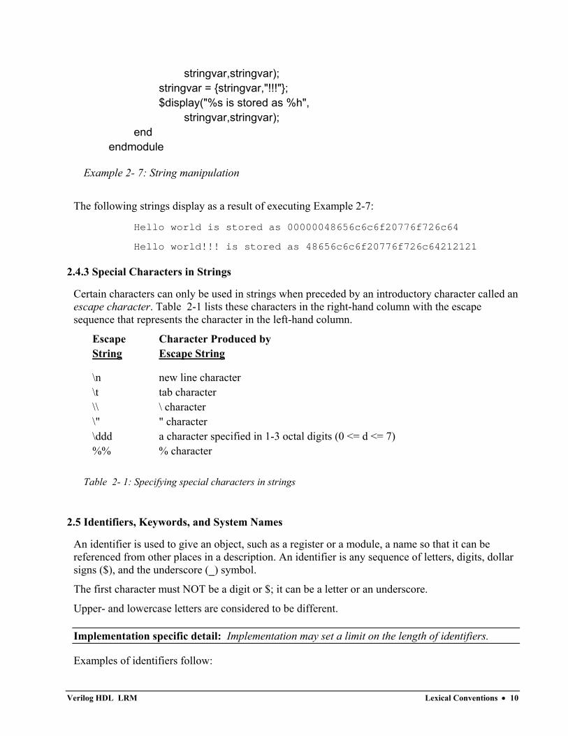
stringvar,stringvar); stringvar = {stringvar,"!!!"}; $display("%s is stored as %h", stringvar,stringvar); end endmodule
Example 2- 7: String manipulation
The following strings display as a result of executing Example 2-7:
Hello world is stored as 00000048656c6c6f20776f726c64
Hello world!!! is stored as 48656c6c6f20776f726c64212121
2.4.3 Special Characters in Strings
Certain characters can only be used in strings when preceded by an introductory character called an escape character. Table 2-1 lists these characters in the right-hand column with the escape sequence that represents the character in the left-hand column.
Escape Character Produced by String Escape String
\n new line character \t tab character \\ \ character \" " character \ddd a character specified in 1-3 octal digits (0 <= d <= 7) %% % character
Table 2- 1: Specifying special characters in strings
2.5 Identifiers, Keywords, and System Names
An identifier is used to give an object, such as a register or a module, a name so that it can be referenced from other places in a description. An identifier is any sequence of letters, digits, dollar signs ($), and the underscore (_) symbol.
The first character must NOT be a digit or $; it can be a letter or an underscore.
Upper- and lowercase letters are considered to be different.
Implementation specific detail: Implementation may set a limit on the length of identifiers.
Examples of identifiers follow:
Verilog HDL LRM Lexical Conventions • 10
shiftreg_a
busa_index
error_condition
merge_ab
_bus3
n$657
2.5.1 Escaped Identifiers
Escaped identifiers start with the backslash character (\) and provide a means of including any of the printable ASCII characters in an identifier (the decimal values 33 through 126, or 21 through 7E in hexadecimal). An escaped identifier ends with white space (blank, tab, newline). Neither the leading back-slash character nor the terminating white space is considered to be part of the identifier.
The primary application of escaped identifiers is for translators from other hardware description languages and CAE systems, where special characters may be allowed in identifiers. Escaped identifiers should not be used under normal circumstances.
Examples of escaped identifiers follow:
\busa+index
\-clock
\***error-condition***
\net1/\net2
\{a,b}
\a*(b+c)
Please note: Remember to terminate escaped identifiers with white space, otherwise characters that should follow the identifier are considered as part of it.
Verilog HDL LRM Lexical Conventions • 11
2.5.2 Keywords
Keywords are predefined non-escaped identifiers that are used to define the language constructs. A Verilog HDL keyword preceded by an escape character is not interpreted as a keyword.
All keywords are defined in lowercase only and therefore must be typed in lowercase in source files. ( Appendix F, Keywords, gives a list of all keywords defined.)
2.5.3 The $keyword Construct
The $ character introduces a language construct that enables you to develop user-defined tasks and functions. Tools interpret the name following the $ as a system task or function. The syntax for a system task or function is as follows:
<name_of_system_task> <name_of_system_function>
::=$<SYSTEM_IDENTIFIER> ; ||=$<SYSTEM_IDENTIFIER> (<parameter><,<parameter>>*);
Syntax 2- 1: Syntax for system tasks and functions
Any valid identifier, including keywords already in use in contexts other than this construct—for example, a compiler directive name—can be used as a system task name. Appendix D lists all of the keywords used as names of system tasks and functions. Appendix B describes some of the more useful tasks and functions. The $keyword construct is part of the Verilog Language. The individual system tasks and functions implemented with the $keyword construct are not part of the Verilog language.
The following are examples of system task names:
$display ("display a message");
$finish;
2.5.4 The `keyword Construct
The ` character (the ASCII value 60, called open quote or accent grave) introduces a language construct used by tools to implement compiler directives. The compiler behavior dictated by a compiler directive takes effect as soon as the compiler reads the directive. The directive remains in effect for the rest of the compilation unless a different compiler directive specifies otherwise. A compiler directive in one description file can therefore control compilation behavior in multiple description files. Appendix C describes some compiler directives. Appendix E lists all the keywords used as names of compiler directives. The `keyword construct is part of the Verilog Language. The individual system tasks and functions implemented with the `keyword construct are not part of the Verilog language.
An example of a compiler directive follows:
Verilog HDL LRM Lexical Conventions • 12
`define wordsize 8
2.6 Text Substitutions
A text macro substitution facility has been provided so that meaningful names can be used to represent commonly used pieces of text. For example, in the situation where a constant number is repetitively used throughout a description, a text macro would be useful in that only one place in the source description would need to be altered if the value of the constant needed to be changed. Text macros can also be defined and used in the interactive mode, where they can be helpful for predefining those interactive commands that you use often.
The syntax for text macro definitions is as follows:
<text_macro_definition> ::= `define <text_macro_name> <MACRO_TEXT>
<text_macro_name> ::= <IDENTIFIER>
Syntax 2- 2: Syntax for <text_macro_definition>
<MACRO_TEXT> is any arbitrary text specified on the same line as the <text_macro_name>. If a one-line comment (that is, a comment specified with the characters //) is included in the text, then the comment does not become part of the text substituted. The text for <MACRO_TEXT> can be blank, in which case the text macro is defined to be empty and no text is substituted when the macro is used.
The syntax for using a text macro is as follows:
<text_macro_usage> ::=`<text_macro_name>
Syntax 2- 3: Syntax for <text_macro_usage>
Once a text macro name has been defined (that is, assigned <MACRO_TEXT>), it can be used anywhere in a source description or in an interactive command; that is, there are no scope restrictions. However, to use a text macro the compiler directive symbol ` (open quote, also known as “accent grave”) must precede the text macro name.
Example 2-8 shows two definitions of macro text and a use of each of the defined macros.
`define wordsize 8 reg [1:`wordsize] data;
`define typ_nand nand #5 // define a nand w/typical delay `typ_nand g121 (q21, n10, n11);
Example 2- 8: Using macro text
Verilog HDL LRM Lexical Conventions • 13
The text specified for <MACRO_TEXT> must not be split across the following lexical tokens:
• comments
• numbers
• strings
• identifiers
• keywords
• double or triple character operators
For example, the following is illegal syntax in the Verilog language because it is split across a string:
`define first_half "start of string
$display(`first_half end of string");
Note that the word define is known as a compiler directive keyword, and is not part of the normal set of keywords. Thus, normal identifiers in a Verilog HDL source description can be the same as compiler directive keywords (though this is not recommended). If you develop compiler directives, be aware of the following pitfall:
• If you implement the compiler directive `foo and implement the directive `define, then if you write `define foo, the meaning of `foo is ambiguous.
• Text macro names may not be the same as compiler directive keywords.
• Text macro names can re-use names being used as ordinary identifiers. For example, signal_name and `signal_name are different. Redefinition of text macros is allowed; the latest definition of a particular text macro read by the compiler prevails when the macro name is encountered in the source text.
Verilog HDL LRM Lexical Conventions • 14
Data Types
3.0 Data Types Overview
The set of Verilog HDL data types is designed to represent the data storage and transmission elements found in digital hardware.
3.1 Value Set
The Verilog HDL value set consists of four basic values:
0 - represents a logic zero, or false condition
1 - represents a logic one, or true condition
x - represents an unknown logic value
z - represents a high-impedance state
The values 0 and 1 are logical complements of one another.
When the z value is present at the input of a gate, or when it is encountered in an expression, the effect is usually the same as an x value. Notable exceptions are the MOS primitives, which can pass the z value.
Almost all of the data types in the Verilog language store all four basic values. The exceptions are the event type, which has no storage, and the trireg net data type, which retains its first state when all of its drivers go to the high impedance value, and z. All bits of vectors can be independently set to one of the four basic values.
The language includes strength information in addition to the basic value information for scalar net variables. This is described in detail in Chapter 6, 6.10 Logic Strength Modeling.
3.2 Registers and Nets
There are two main groups of data types: the register data types and the net data types. These two groups differ in the way that they are assigned and hold values. They also represent different hardware structures.
3.2.1 Nets
The net data types represent physical connections between structural entities, such as gates. A net does not store a value (except for the trireg net, discussed in Section 3.7.3). Instead, it must be driven by a driver, such as a gate or a continuous assignment. See Chapter 6, "Gate and Switch Level Modeling", and Chapter 5, "Assignments", for definitions of these constructs. If no driver is connected to a net, its value will be high-impedance (z)—unless the net is a trireg, in which case, it holds to the previously driven value.
Verilog HDL LRM Data Types • 15
3.2.2 Registers
A register is an abstraction of a data storage element. The keyword for the register data type is reg. A register stores a value from one assignment to the next. An assignment statement in a procedure acts as a trigger that changes the value in the data storage element. The Verilog language has powerful constructs that allow you to control when and if these assignment statements are executed. These control constructs are used to describe hardware trigger conditions, such as the rising edge of a clock, and decision-making logic, such as a multiplexer. Chapter 8, 8.1 Behavioral Model Overview, describes these control constructs.
The default initialization value for a reg data type is the unknown value, x.
CAUTION
Registers can be assigned negative values, but, when a register is an operand in an expression, its value is treated as an unsigned (positive) value. For example, a minus one in a four-bit register functions as the number 15 if the register is an expression operand. For more information, see "4.1.2 Numeric Conventions in Expressions".
3.2.3 Declaration Syntax
The syntax for net and register declarations is as follows:
<net_declaration> ::= <NETTYPE> <expandrange>? <delay>? <list_of_variables> ; ||= trireg <charge_strength>? <expandrange>? <delay>? <list_of_variables> ; ||= <NETTYPE> <drive_strength>? <expandrange>? <delay>?
<list_of_assignments> ;
<reg_declaration> ::= reg <range>? <list_of_register_variables> ;
<list_of_variables> ::= <name_of_variable> <,<name_of_variable>>*
<name_of_variable> ::= <IDENTIFIER>
<list_of_register_variables> ::= <register_variable> <,<register_variable>>*
<register_variable> ::= <name_of_register>
<name_of_register>
Verilog HDL LRM Data Types • 16
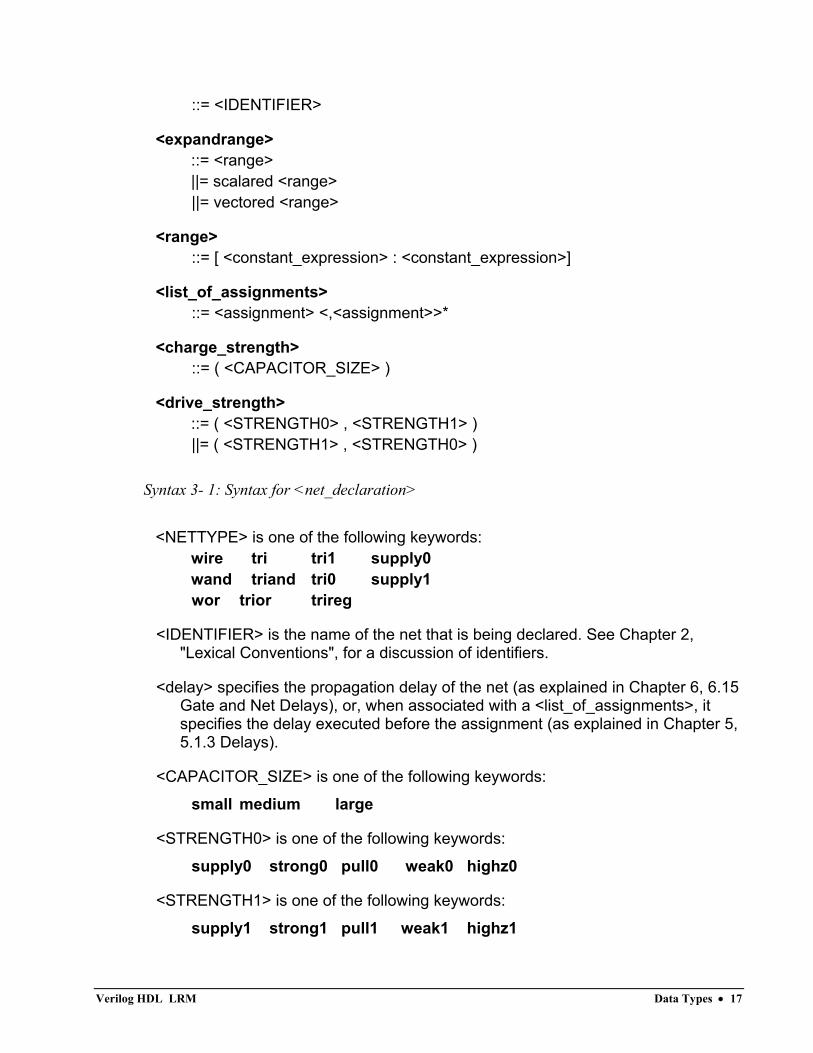
::= <IDENTIFIER>
<expandrange> ::= <range> ||= scalared <range> ||= vectored <range>
<range> ::= [ <constant_expression> : <constant_expression>]
<list_of_assignments> ::= <assignment> <,<assignment>>*
<charge_strength> ::= ( <CAPACITOR_SIZE> )
<drive_strength> ::= ( <STRENGTH0> , <STRENGTH1> ) ||= ( <STRENGTH1> , <STRENGTH0> )
Syntax 3- 1: Syntax for <net_declaration>
<NETTYPE> is one of the following keywords: wire tri tri1 supply0 wand triand tri0 supply1 wor trior trireg
<IDENTIFIER> is the name of the net that is being declared. See Chapter 2, "Lexical Conventions", for a discussion of identifiers.
<delay> specifies the propagation delay of the net (as explained in Chapter 6, 6.15 Gate and Net Delays), or, when associated with a <list_of_assignments>, it specifies the delay executed before the assignment (as explained in Chapter 5, 5.1.3 Delays).
<CAPACITOR_SIZE> is one of the following keywords:
small medium large
<STRENGTH0> is one of the following keywords:
supply0 strong0 pull0 weak0 highz0
<STRENGTH1> is one of the following keywords:
supply1 strong1 pull1 weak1 highz1
Verilog HDL LRM Data Types • 17
Syntax 3- 2: Definitions for <net_declaration> syntax
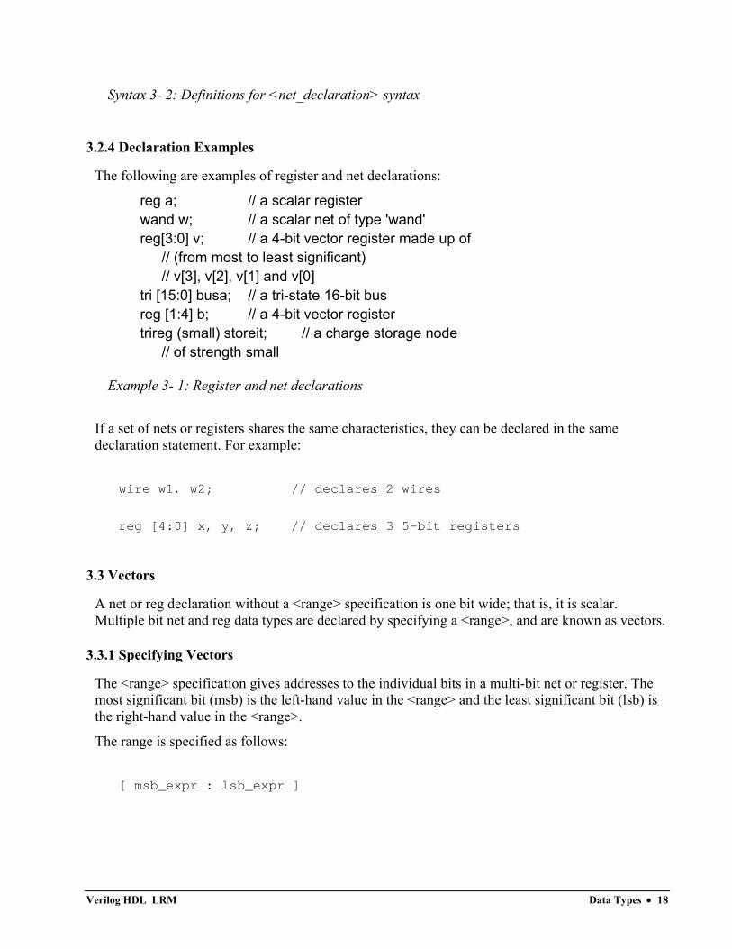
3.2.4 Declaration Examples
The following are examples of register and net declarations:
reg a; // a scalar register wand w; // a scalar net of type 'wand' reg[3:0] v; // a 4-bit vector register made up of // (from most to least significant) // v[3], v[2], v[1] and v[0] tri [15:0] busa; // a tri-state 16-bit bus reg [1:4] b; // a 4-bit vector register trireg (small) storeit; // a charge storage node // of strength small
Example 3- 1: Register and net declarations
If a set of nets or registers shares the same characteristics, they can be declared in the same declaration statement. For example:
wire w1, w2; // declares 2 wires
reg [4:0] x, y, z; // declares 3 5-bit registers
3.3 Vectors
A net or reg declaration without a <range> specification is one bit wide; that is, it is scalar. Multiple bit net and reg data types are declared by specifying a <range>, and are known as vectors.
3.3.1 Specifying Vectors
The <range> specification gives addresses to the individual bits in a multi-bit net or register. The most significant bit (msb) is the left-hand value in the <range> and the least significant bit (lsb) is the right-hand value in the <range>.
The range is specified as follows:
[ msb_expr : lsb_expr ]
Verilog HDL LRM Data Types • 18
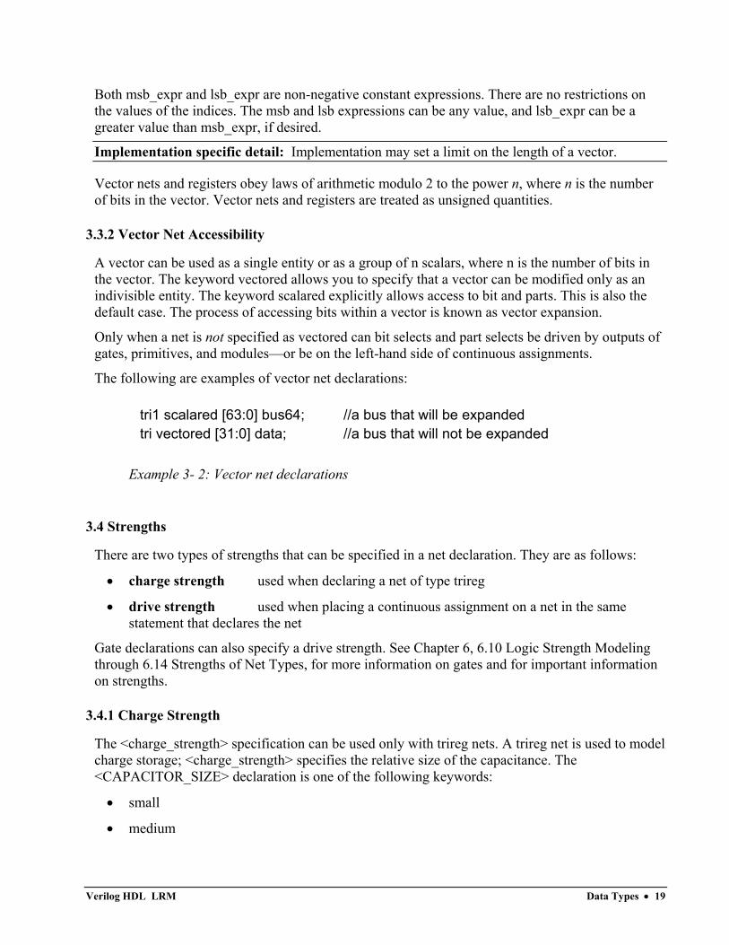
Both msb_expr and lsb_expr are non-negative constant expressions. There are no restrictions on the values of the indices. The msb and lsb expressions can be any value, and lsb_expr can be a greater value than msb_expr, if desired.
Implementation specific detail: Implementation may set a limit on the length of a vector.
Vector nets and registers obey laws of arithmetic modulo 2 to the power n, where n is the number of bits in the vector. Vector nets and registers are treated as unsigned quantities.
3.3.2 Vector Net Accessibility
A vector can be used as a single entity or as a group of n scalars, where n is the number of bits in the vector. The keyword vectored allows you to specify that a vector can be modified only as an indivisible entity. The keyword scalared explicitly allows access to bit and parts. This is also the default case. The process of accessing bits within a vector is known as vector expansion.
Only when a net is not specified as vectored can bit selects and part selects be driven by outputs of gates, primitives, and modules—or be on the left-hand side of continuous assignments.
The following are examples of vector net declarations:
tri1 scalared [63:0] bus64; //a bus that will be expanded tri vectored [31:0] data; //a bus that will not be expanded
Example 3- 2: Vector net declarations
3.4 Strengths
There are two types of strengths that can be specified in a net declaration. They are as follows:
• charge strength used when declaring a net of type trireg
• drive strength used when placing a continuous assignment on a net in the same statement that declares the net
Gate declarations can also specify a drive strength. See Chapter 6, 6.10 Logic Strength Modeling through 6.14 Strengths of Net Types, for more information on gates and for important information on strengths.
3.4.1 Charge Strength
The <charge_strength> specification can be used only with trireg nets. A trireg net is used to model charge storage; <charge_strength> specifies the relative size of the capacitance. The <CAPACITOR_SIZE> declaration is one of the following keywords:
• small
• medium
Verilog HDL LRM Data Types • 19
• large
When no size is specified in a trireg declaration, its size is medium.
The following is a syntax example of a strength declaration:
trireg (small) st1 ;
A trireg net can model a charge storage node whose charge decays over time. The simulation time of a charge decay is specified in the trireg net’s delay specification (see "6.15.2 trireg Net Charge Decay").
3.4.2 Drive Strength
The <drive_strength> specification allows a continuous assignment to be placed on a net in the same statement that declares that net. See Chapter 5, 5.1.4 Strength, for more details.
Net strength properties are described in detail in Chapter 6, 6.10 Logic Strength Modeling through 6.14 Strengths of Net Types.
3.5 Implicit Declarations
The syntax shown in Section 3.2.3, Declaration Syntax, is used to explicitly declare variables. In the absence of an explicit declaration of a variable, statements for gate, user-defined primitive, and module instantiations assume an implicit variable declaration. This happens if you do the following: in the terminal list of an instance of a gate, a user-defined primitive, or a module, specify a variable that has not been explicitly declared previously in one of the declaration statements of the instantiating module.
These implicitly declared variables are scalar nets of type wire.
See Appendix C, C.2 `default_nettype, for a discussion of control of the type for implicitly declared nets with the ‘default_nettype compiler directive.
3.6 Net Initialization
The default initialization value for a net is the value z. Nets with drivers assume the output value of their drivers, which defaults to x. The trireg net is an exception to these statements. The trireg defaults to the value x, with the strength specified in the net declaration (small, medium, or large).
3.7 Net Types
There are several distinct types of nets. Each is described in the sections that follow.
3.7.1 wire and tri Nets
The wire and tri nets connect elements. The net types wire and tri are identical in their syntax and functions; two names are provided so that the name of a net can indicate the purpose of the net in
Verilog HDL LRM Data Types • 20
that model. A wire net is typically used for nets that are driven by a single gate or continuous assignment. The tri net type might be used where multiple drivers drive a net.
Logical conflicts from multiple sources on a wire or a tri net result in unknown values unless the net is controlled by logic strength.
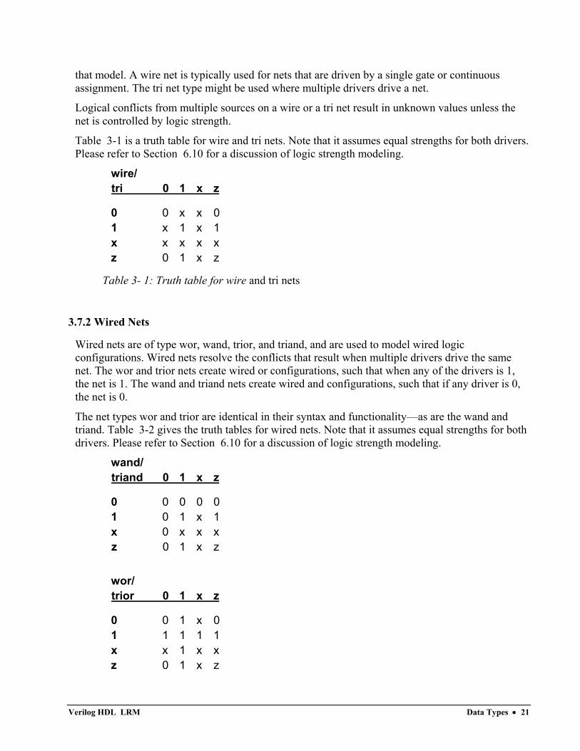
Table 3-1 is a truth table for wire and tri nets. Note that it assumes equal strengths for both drivers. Please refer to Section 6.10 for a discussion of logic strength modeling.
wire/ tri 0 1 x z
0 0 x x 0 1 x 1 x 1 x x x x x z 0 1 x z
Table 3- 1: Truth table for wire and tri nets
3.7.2 Wired Nets
Wired nets are of type wor, wand, trior, and triand, and are used to model wired logic configurations. Wired nets resolve the conflicts that result when multiple drivers drive the same net. The wor and trior nets create wired or configurations, such that when any of the drivers is 1, the net is 1. The wand and triand nets create wired and configurations, such that if any driver is 0, the net is 0.
The net types wor and trior are identical in their syntax and functionality—as are the wand and triand. Table 3-2 gives the truth tables for wired nets. Note that it assumes equal strengths for both drivers. Please refer to Section 6.10 for a discussion of logic strength modeling.
wand/ triand 0 1 x z
0 0 0 0 0 1 0 1 x 1 x 0 x x x z 0 1 x z
wor/ trior 0 1 x z
0 0 1 x 0 1 1 1 1 1 x x 1 x x z 0 1 x z
Verilog HDL LRM Data Types • 21
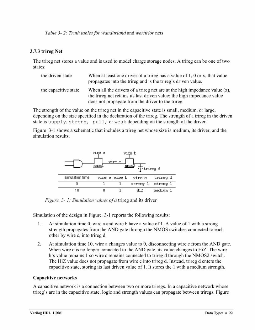
Table 3- 2: Truth tables for wand/triand and wor/trior nets
3.7.3 trireg Net
The trireg net stores a value and is used to model charge storage nodes. A trireg can be one of two states:
the driven state When at least one driver of a trireg has a value of 1, 0 or x, that value propagates into the trireg and is the trireg’s driven value.
the capacitive state When all the drivers of a trireg net are at the high impedance value (z), the trireg net retains its last driven value; the high impedance value does not propagate from the driver to the trireg.
The strength of the value on the trireg net in the capacitive state is small, medium, or large, depending on the size specified in the declaration of the trireg. The strength of a trireg in the driven state is supply, strong, pull, or weak depending on the strength of the driver.
Figure 3-1 shows a schematic that includes a trireg net whose size is medium, its driver, and the simulation results.
Figure 3- 1: Simulation values of a trireg and its driver
Simulation of the design in Figure 3-1 reports the following results:
1. At simulation time 0, wire a and wire b have a value of 1. A value of 1 with a strong strength propagates from the AND gate through the NMOS switches connected to each other by wire c, into trireg d.
2. At simulation time 10, wire a changes value to 0, disconnecting wire c from the AND gate. When wire c is no longer connected to the AND gate, its value changes to HiZ. The wire b’s value remains 1 so wire c remains connected to trireg d through the NMOS2 switch. The HiZ value does not propagate from wire c into trireg d. Instead, trireg d enters the capacitive state, storing its last driven value of 1. It stores the 1 with a medium strength.
Capacitive networks
A capacitive network is a connection between two or more triregs. In a capacitive network whose trireg’s are in the capacitive state, logic and strength values can propagate between triregs. Figure
Verilog HDL LRM Data Types • 22
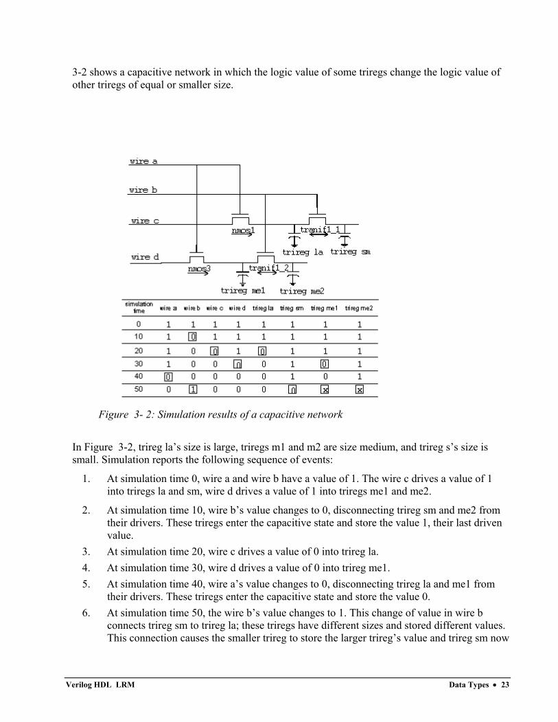
3-2 shows a capacitive network in which the logic value of some triregs change the logic value of other triregs of equal or smaller size.
Figure 3- 2: Simulation results of a capacitive network
In Figure 3-2, trireg la’s size is large, triregs m1 and m2 are size medium, and trireg s’s size is small. Simulation reports the following sequence of events:
1. At simulation time 0, wire a and wire b have a value of 1. The wire c drives a value of 1 into triregs la and sm, wire d drives a value of 1 into triregs me1 and me2.
2. At simulation time 10, wire b’s value changes to 0, disconnecting trireg sm and me2 from their drivers. These triregs enter the capacitive state and store the value 1, their last driven value.
3. At simulation time 20, wire c drives a value of 0 into trireg la. 4. At simulation time 30, wire d drives a value of 0 into trireg me1. 5. At simulation time 40, wire a’s value changes to 0, disconnecting trireg la and me1 from
their drivers. These triregs enter the capacitive state and store the value 0. 6. At simulation time 50, the wire b’s value changes to 1. This change of value in wire b
connects trireg sm to trireg la; these triregs have different sizes and stored different values. This connection causes the smaller trireg to store the larger trireg’s value and trireg sm now
Verilog HDL LRM Data Types • 23
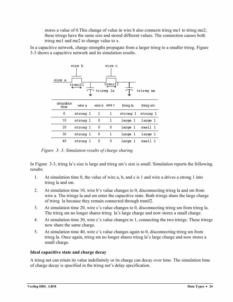
stores a value of 0.This change of value in wire b also connects trireg me1 to trireg me2; these triregs have the same size and stored different values. The connection causes both trireg me1 and me2 to change value to x.
In a capacitive network, charge strengths propagate from a larger trireg to a smaller trireg. Figure 3-3 shows a capacitive network and its simulation results.
Figure 3- 3: Simulation results of charge sharing
In Figure 3-3, trireg la’s size is large and trireg sm’s size is small. Simulation reports the following results:
1. At simulation time 0, the value of wire a, b, and c is 1 and wire a drives a strong 1 into trireg la and sm.
2. At simulation time 10, wire b’s value changes to 0, disconnecting trireg la and sm from wire a. The triregs la and sm enter the capacitive state. Both triregs share the large charge of trireg la because they remain connected through tranif2.
3. At simulation time 20, wire c’s value changes to 0, disconnecting trireg sm from trireg la. The trireg sm no longer shares trireg la’s large charge and now stores a small charge.
4. At simulation time 30, wire c’s value changes to 1, connecting the two triregs. These triregs now share the same charge.
5. At simulation time 40, wire c’s value changes again to 0, disconnecting trireg sm from trireg la. Once again, trireg sm no longer shares trireg la’s large charge and now stores a small charge.
Ideal capacitive state and charge decay
A trireg net can retain its value indefinitely or its charge can decay over time. The simulation time of charge decay is specified in the trireg net’s delay specification.
Verilog HDL LRM Data Types • 24
3.7.4 tri0 and tri1 Nets
The tri0 and tri1 nets model nets with resistive pulldown and resistive pullup devices on them. When no driver drives a tri0 net, its value is 0. When no driver drives a tri1 net, its value is 1. The strength of this value is pull. See Chapter 6, 6.10 Logic Strength Modeling through 6.14 Strengths of Net Types, for a description of strength modeling.
3.7.5 supply Nets
The supply0 and supply1 nets model the power supplies in a circuit. The supply0 nets are used to model Vss (ground) and supply1 nets are used to model Vdd or Vcc (power). These nets should never be connected to the output of a gate or continuous assignment, because the strength they possess will override the driver. They have supply0 or supply1 strengths.
3.8 Memories
The Verilog HDL models memories as an array of register variables. These arrays can be used to model read-only memories (ROMs), random access memories (RAMs), and register files. Each register in the array is known as an element or word and is addressed by a single array index. There are no multiple dimension arrays in the Verilog Language.
Memories are declared in register declaration statements by specifying the element address range after the declared identifier. Syntax 3-3 gives the syntax for a register declaration statement. Note that this syntax extends the <register_variable> definition given in Section 3.2.3, Declaration Syntax.
<register_variable> ::= <name_of_register> ||= <name_of_memory> [ <constant_expression> : <constant_expression> ]
<constant_expression> ::=<expression>
<name_of_memory>
::= <IDENTIFIER>
Syntax 3- 3: Syntax for <register_variable>
The following example illustrates a memory declaration:
reg[7:0] mema[0:255];
This example declares a memory called mema consisting of 256 eight-bit registers. The indices are 0 through 255. The expressions that specify the indices of the array must be constant expressions.
Verilog HDL LRM Data Types • 25
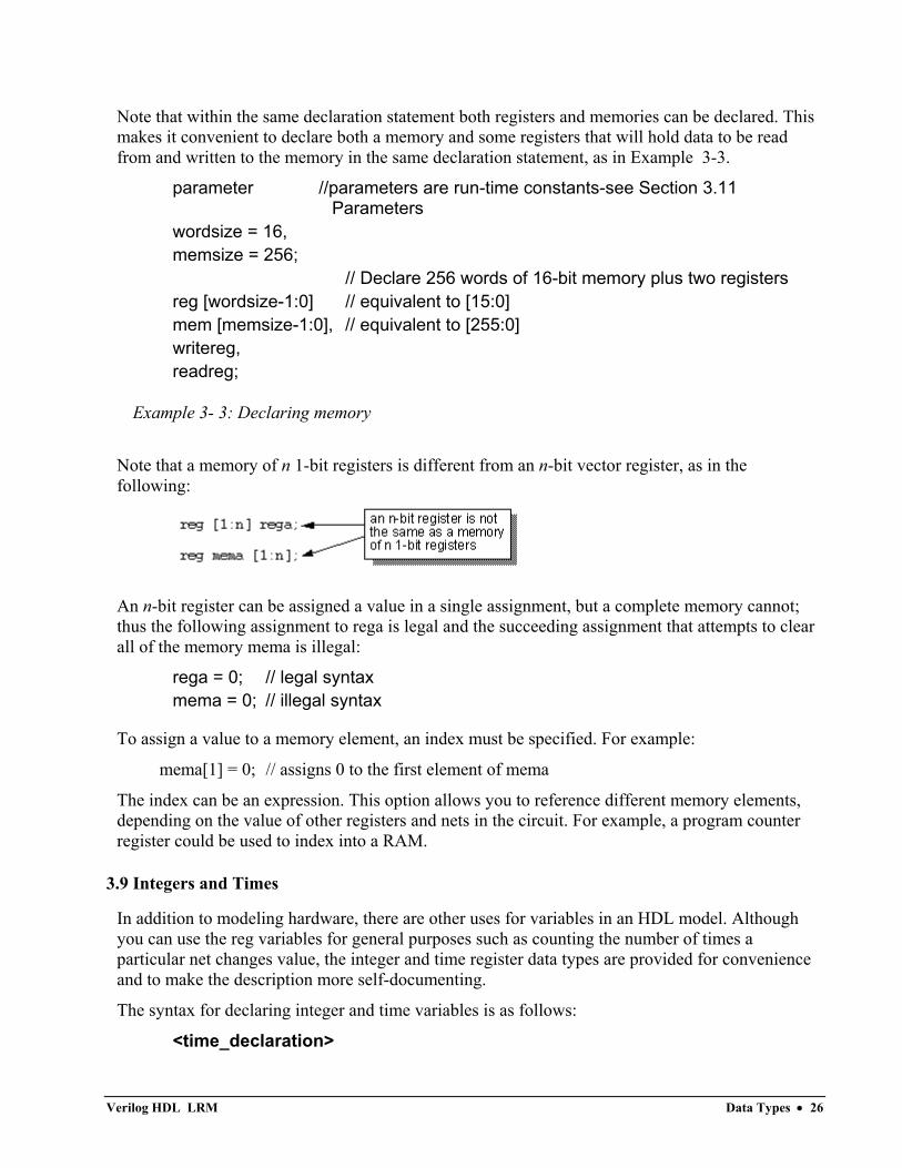
Note that within the same declaration statement both registers and memories can be declared. This makes it convenient to declare both a memory and some registers that will hold data to be read from and written to the memory in the same declaration statement, as in Example 3-3.
parameter //parameters are run-time constants-see Section 3.11 Parameters
wordsize = 16, memsize = 256; // Declare 256 words of 16-bit memory plus two registers reg [wordsize-1:0] // equivalent to [15:0] mem [memsize-1:0], // equivalent to [255:0] writereg, readreg;
Example 3- 3: Declaring memory
Note that a memory of n 1-bit registers is different from an n-bit vector register, as in the following:
An n-bit register can be assigned a value in a single assignment, but a complete memory cannot; thus the following assignment to rega is legal and the succeeding assignment that attempts to clear all of the memory mema is illegal:
rega = 0; // legal syntax mema = 0; // illegal syntax
To assign a value to a memory element, an index must be specified. For example:
mema[1] = 0; // assigns 0 to the first element of mema
The index can be an expression. This option allows you to reference different memory elements, depending on the value of other registers and nets in the circuit. For example, a program counter register could be used to index into a RAM.
3.9 Integers and Times
In addition to modeling hardware, there are other uses for variables in an HDL model. Although you can use the reg variables for general purposes such as counting the number of times a particular net changes value, the integer and time register data types are provided for convenience and to make the description more self-documenting.
The syntax for declaring integer and time variables is as follows:
<time_declaration>
Verilog HDL LRM Data Types • 26
::= time <list_of_register_variables> ;
<integer_declaration> ::= integer <list_of_register_variables> ;
Syntax 3- 4: Syntax for time and integer declarations
The <list_of_register_variables> item is defined in Section 3.2.3, Declaration Syntax.
A time variable is used for storing and manipulating simulation time quantities in situations where timing checks are required and for diagnostics and debugging purposes. This data type is typically used in conjunction with the $time system function (see Appendix B, B.6 Simulation Time—The $time Function). The size of a time variable is 64 bits.
An integer is a general purpose variable used for manipulating quantities that are not regarded as hardware registers.
Implementation specific detail: An implemtation may limit the size of the integer variable, and the time variable.
Arrays of integer and time variables are allowed. They are declared in the same manner as arrays of reg variables, as in the following example:
integer a[1:64]; // an array of 64 integers
time change_history[1:1000]; // an array of 1000 times
The integer and time variables are assigned values in the same manner as reg variables. Procedural assignments are used to trigger their value changes.
Time variables behave the same as 64 bit reg variables. They are unsigned quantities, and unsigned arithmetic is performed on them. In contrast, integer variables are signed quantities. Arithmetic operations performed on integer variables produce 2’s complement results.
3.10 Real Numbers
The Verilog HDL supports real number constants and variables in addition to integers and time variables. The syntax for real numbers is the same as the syntax for register types, and is described in Section 3.10.1. Except for the following restrictions, real number variables can be used in the same places that integers and time variables are used.
• Not all Verilog HDL operators can be used with real number values. See Table 4-2 in Section 4.1 Operators for lists of valid and invalid operators for real numbers.
• Ranges are not allowed on real number variable declarations.
• Real number variables default to an initial value of zero.
Verilog HDL LRM Data Types • 27
3.10.1 Declaration Syntax for Real Numbers
The syntax for declaring real number variables is as follows:
<real_declaration> ::=real<list_of_variables>;
Syntax 3- 5: Syntax for real number variable declarations
The <list_of_variables> item is defined in Section 3.2.3 Declaration Syntax.
3.10.2 Specifying Real Numbers
Real numbers can be specified in either decimal notation (for example, 14.72) or in scientific notation (for example, 39e8, which indicates 39 multiplied by 10 to the 8th power). Real numbers expressed with a decimal point must have at least one digit on each side of the decimal point.
The following are some examples of valid real numbers in the Verilog language:
1.2 0.1 2394.26331 1.2E12 (the exponent symbol can be e or E) 1.30e-2 0.1e-0 23E10 29E-2 236.123_763_e-12 (underscores are ignored)
The following are invalid real numbers in the Verilog HDL because they do not have a digit to the left of the decimal point:
.12
.3E3
.2e-7
3.10.3 Operators and Real Numbers
The result of using logical or relational operators on real numbers is a single-bit scalar value. Not all Verilog operators can be used with real number expressions. Table 4-2 in Section 4.1 lists the valid operators for use with real numbers. Real number constants and real number variables are also prohibited in the following contexts:
• edge descriptors (posedge, negedge) applied to real number variables
• bit-select or part-select references of variables declared as real
• real number index expressions of bit-select or part-select references of vectors
Verilog HDL LRM Data Types • 28
• real number memories (arrays of real numbers)
3.10.4 Conversion
The Verilog language converts real numbers to integers by rounding a real number to the nearest integer, rather than by truncating it. For example, the real numbers 35.7 and 35.5 both become 36 when converted to an integer and 35.2 becomes 35. Implicit conversion takes place when you assign a real to an integer.
See Appendix B, B.8 Functions and Tasks for Reals, for a discussion of system tasks that perform explicit conversion.
3.11 Parameters
Verilog parameters do not belong to either the register or the net group. Parameters are not variables, they are constants. The syntax for parameter declarations is as follows:
<parameter_declaration> ::= parameter <list_of_assignments> ;
Syntax 3- 6: Syntax for <parameter_declaration>
Implementation specific detail: Some implementations accept a range specification on the parameter declaration.
The <list_of_assignments> is a comma-separated list of assignments, where the right-hand side of the assignment must be a constant expression, that is, an expression containing only constant numbers and previously defined parameters. Example 3-4 shows examples of parameter declarations:
parameter msb = 7; // defines msb as a constant value 7
parameter e = 25, f = 9; // defines two constant numbers
parameter r = 5.7; //declares r as a 'real' parameter
parameter byte_size = 8, byte_mask = byte_size - 1;
parameter average_delay = (r + f) / 2;
Example 3- 4: Parameter declarations
Even though they represent constants, Verilog parameters can be modified at compilation time to have values that are different from those specified in the declaration assignment. This allows you to customize module instances. You can modify the parameter with the defparam statement, or you can modify the parameter in the module instance statement. Typical uses of parameters are to
Verilog HDL LRM Data Types • 29
specify delays and width of variables. See Chapter 12, 12.2 Overriding Module Parameter Values, for complete details on parameter value assignment.
Verilog HDL LRM Data Types • 30
Expressions
4.0 Expressions Overview
This chapter describes the operators and operands available in the Verilog HDL, and how to use them to form expressions.
An expression is a construct that combines operands with operators to produce a result that is a function of the values of the operands and the semantic meaning of the operator. Alternatively, an expression is any legal operand—for example, a net bit-select. Wherever a value is needed in a Verilog HDL statement, an expression can be given. However, several statement constructs limit an expression to a constant expression. A constant expression consists of constant numbers and predefined parameter names only, but can use any of the operators defined in Table 4-1.
For their use in expressions, integer and time data types share the same traits as the data type reg. Descriptions pertaining to register usage apply to integers and times as well.
An operand can be one of the following:
• number (including real)
• net
• register, integer, time
• net bit-select
• register bit-select
• net part-select
• register part-select
• memory element
• a call to a user-defined function or system defined function that returns any of the above
4.1 Operators
The symbols for the Verilog HDL operators are similar to those in the C language. Table 4-1 lists these operators.
Verilog Language Operators
{} concatenation + - * / arithmetic % modulus > >= < <= relational ! logical negation && logical and || logical or
Verilog HDL LRM Expressions • 31
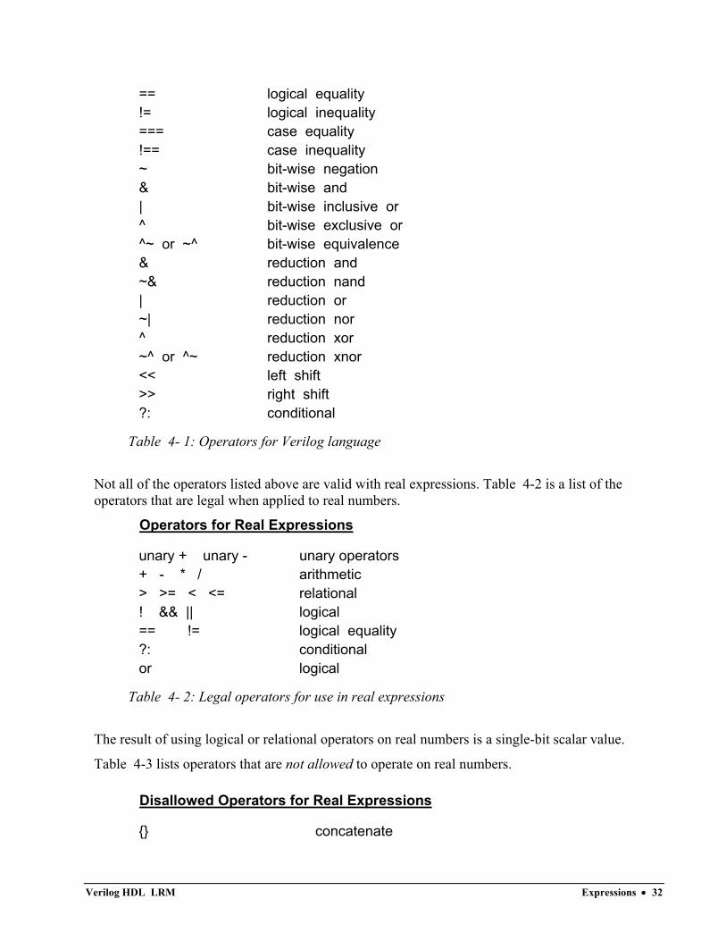
== logical equality != logical inequality === case equality !== case inequality ~ bit-wise negation & bit-wise and | bit-wise inclusive or ^ bit-wise exclusive or ^~ or ~^ bit-wise equivalence & reduction and ~& reduction nand | reduction or ~| reduction nor ^ reduction xor ~^ or ^~ reduction xnor << left shift >> right shift ?: conditional
Table 4- 1: Operators for Verilog language
Not all of the operators listed above are valid with real expressions. Table 4-2 is a list of the operators that are legal when applied to real numbers.
Operators for Real Expressions
unary + unary - unary operators + - * / arithmetic > >= < <= relational ! && || logical == != logical equality ?: conditional or logical
Table 4- 2: Legal operators for use in real expressions
The result of using logical or relational operators on real numbers is a single-bit scalar value.
Table 4-3 lists operators that are not allowed to operate on real numbers.
Disallowed Operators for Real Expressions
{} concatenate
Verilog HDL LRM Expressions • 32
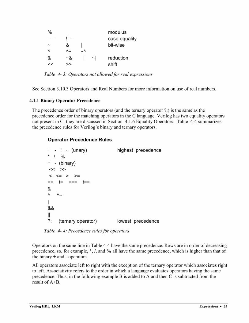
% modulus === !== case equality ~ & | bit-wise ^ ^~ ~^ & ~& | ~| reduction << >> shift
Table 4- 3: Operators not allowed for real expressions
See Section 3.10.3 Operators and Real Numbers for more information on use of real numbers.
4.1.1 Binary Operator Precedence
The precedence order of binary operators (and the ternary operator ?:) is the same as the precedence order for the matching operators in the C language. Verilog has two equality operators not present in C; they are discussed in Section 4.1.6 Equality Operators. Table 4-4 summarizes the precedence rules for Verilog’s binary and ternary operators.
Operator Precedence Rules
+ - ! ~ (unary) highest precedence * / % + - (binary) << >> < <= > >= == != === !== & ^ ^~ | && || ?: (ternary operator) lowest precedence
Table 4- 4: Precedence rules for operators
Operators on the same line in Table 4-4 have the same precedence. Rows are in order of decreasing precedence, so, for example, *, /, and % all have the same precedence, which is higher than that of the binary + and - operators.
All operators associate left to right with the exception of the ternary operator which associates right to left. Associativity refers to the order in which a language evaluates operators having the same precedence. Thus, in the following example B is added to A and then C is subtracted from the result of A+B.
Verilog HDL LRM Expressions • 33
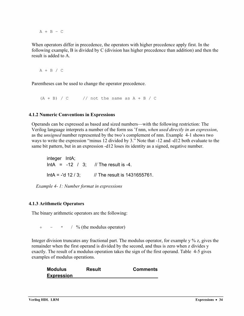
A + B - C
When operators differ in precedence, the operators with higher precedence apply first. In the following example, B is divided by C (division has higher precedence than addition) and then the result is added to A.
A + B / C
Parentheses can be used to change the operator precedence.
(A + B) / C // not the same as A + B / C
4.1.2 Numeric Conventions in Expressions
Operands can be expressed as based and sized numbers—with the following restriction: The Verilog language interprets a number of the form sss ’f nnn, when used directly in an expression, as the unsigned number represented by the two’s complement of nnn. Example 4-1 shows two ways to write the expression “minus 12 divided by 3.” Note that -12 and -d12 both evaluate to the same bit pattern, but in an expression -d12 loses its identity as a signed, negative number.
integer IntA; IntA = -12 / 3; // The result is -4.
IntA = -'d 12 / 3; // The result is 1431655761.
Example 4- 1: Number format in expressions
4.1.3 Arithmetic Operators
The binary arithmetic operators are the following:
+ - * / % (the modulus operator)
Integer division truncates any fractional part. The modulus operator, for example y % z, gives the remainder when the first operand is divided by the second, and thus is zero when z divides y exactly. The result of a modulus operation takes the sign of the first operand. Table 4-5 gives examples of modulus operations.
Modulus Result Comments Expression
Verilog HDL LRM Expressions • 34
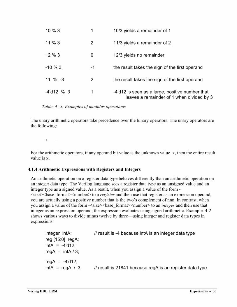
10 % 3 1 10/3 yields a remainder of 1 11 % 3 2 11/3 yields a remainder of 2 12 % 3 0 12/3 yields no remainder -10 % 3 -1 the result takes the sign of the first operand 11 % -3 2 the result takes the sign of the first operand -4'd12 % 3 1 -4'd12 is seen as a large, positive number that
leaves a remainder of 1 when divided by 3
Table 4- 5: Examples of modulus operations
The unary arithmetic operators take precedence over the binary operators. The unary operators are the following:
+ -
For the arithmetic operators, if any operand bit value is the unknown value x, then the entire result value is x.
4.1.4 Arithmetic Expressions with Registers and Integers
An arithmetic operation on a register data type behaves differently than an arithmetic operation on an integer data type. The Verilog language sees a register data type as an unsigned value and an integer type as a signed value. As a result, when you assign a value of the form -<size><base_format><number> to a register and then use that register as an expression operand, you are actually using a positive number that is the two’s complement of nnn. In contrast, when you assign a value of the form -<size><base_format><number> to an integer and then use that integer as an expression operand, the expression evaluates using signed arithmetic. Example 4-2 shows various ways to divide minus twelve by three—using integer and register data types in expressions.
integer intA; // result is -4 because intA is an integer data type reg [15:0] regA; intA = -4'd12; regA = intA / 3;
regA = -4'd12; intA = regA / 3; // result is 21841 because regA is an register data type
Verilog HDL LRM Expressions • 35
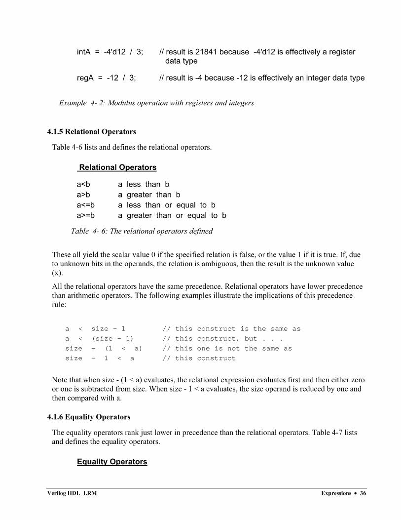
intA = -4'd12 / 3; // result is 21841 because -4'd12 is effectively a register data type
regA = -12 / 3; // result is -4 because -12 is effectively an integer data type
Example 4- 2: Modulus operation with registers and integers
4.1.5 Relational Operators
Table 4-6 lists and defines the relational operators.
Relational Operators
a<b a less than b a>b a greater than b a<=b a less than or equal to b a>=b a greater than or equal to b
Table 4- 6: The relational operators defined
These all yield the scalar value 0 if the specified relation is false, or the value 1 if it is true. If, due to unknown bits in the operands, the relation is ambiguous, then the result is the unknown value (x).
All the relational operators have the same precedence. Relational operators have lower precedence than arithmetic operators. The following examples illustrate the implications of this precedence rule:
a < size - 1 // this construct is the same as
a < (size - 1) // this construct, but . . .
size - (1 < a) // this one is not the same as
size - 1 < a // this construct
Note that when size - (1 < a) evaluates, the relational expression evaluates first and then either zero or one is subtracted from size. When size - 1 < a evaluates, the size operand is reduced by one and then compared with a.
4.1.6 Equality Operators
The equality operators rank just lower in precedence than the relational operators. Table 4-7 lists and defines the equality operators.
Equality Operators
Verilog HDL LRM Expressions • 36
a === b a equal to b, including x and z a !== b a not equal to b, including x and z a == b a equal to b, result may be unknown a != b a not equal to b, result may be unknown
Table 4- 7: The equality operators defined
All four equality operators have the same precedence. These four operators compare operands bit for bit, with zero filling if the two operands are of unequal bit-length. As with the relational operators, the result is 0 if false, 1 if true.
For the == and != operators, if either operand contains an x or a z, then the result is the unknown value (x).
For the === and !== operators, the comparison is done just as it is in the procedural case statement. Bits which are x or z are included in the comparison and must match for the result to be true. The result of these operators is always a known value, either 1 or 0.
4.1.7 Logical Operators
The operators logical AND (&&) and logical OR (||) are logical connectives. The result of the evaluation of a logical comparison is one (defined as true), zero (defined as false), or, if the result is ambiguous, then the result is the unknown value (x). For example, if register alpha holds the integer value 237 and beta holds the value zero, then the following examples perform as described:
regA = alpha && beta; // regA is set to 0
regB = alpha || beta; // regB is set to 1
The precedence of && is greater than that of ||, and both are lower than relational and equality operators. The following expression ANDs three sub-expressions without needing any parentheses:
a < size-1 && b != c && index != lastone
However, it is recommended for readability purposes that parentheses be used to show very clearly the precedence intended, as in the following rewrite of the above example:
(a < size-1) && (b != c) && (index != lastone)
A third logical operator is the unary logical negation operator !. The negation operator converts a non-zero or true operand into 0 and a zero or false operand into 1. An ambiguous truth value remains as x. A common use of ! is in constructions like the following:
if (!inword)
Verilog HDL LRM Expressions • 37
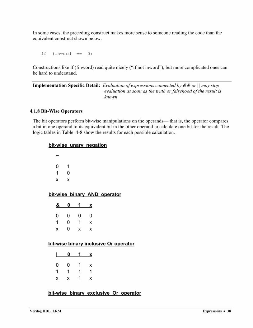
In some cases, the preceding construct makes more sense to someone reading the code than the equivalent construct shown below:
if (inword == 0)
Constructions like if (!inword) read quite nicely (“if not inword”), but more complicated ones can be hard to understand.
Implementation Specific Detail: Evaluation of expressions connected by && or || may stop evaluation as soon as the truth or falsehood of the result is known
4.1.8 Bit-Wise Operators
The bit operators perform bit-wise manipulations on the operands— that is, the operator compares a bit in one operand to its equivalent bit in the other operand to calculate one bit for the result. The logic tables in Table 4-8 show the results for each possible calculation.
bit-wise unary negation
~
0 1 1 0 x x
bit-wise binary AND operator
& 0 1 x
0 0 0 0 1 0 1 x x 0 x x
bit-wise binary inclusive Or operator
| 0 1 x
0 0 1 x 1 1 1 1 x x 1 x
bit-wise binary exclusive Or operator
Verilog HDL LRM Expressions • 38
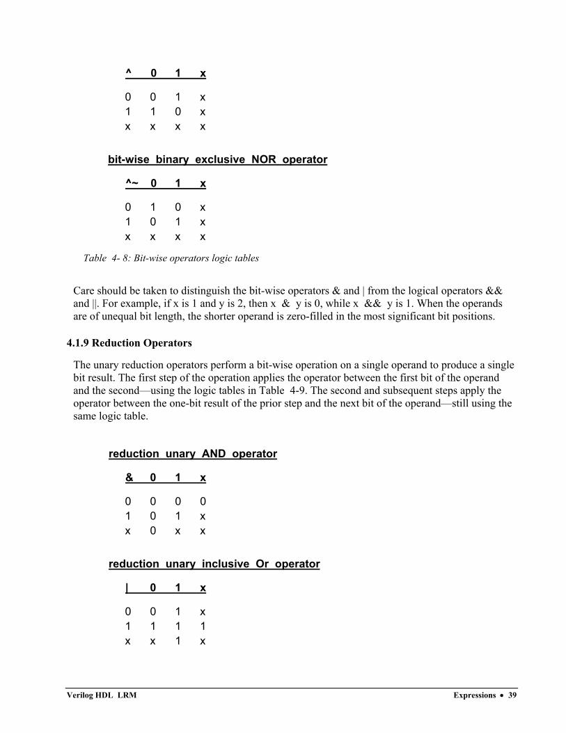
^ 0 1 x
0 0 1 x 1 1 0 x x x x x
bit-wise binary exclusive NOR operator
^~ 0 1 x
0 1 0 x 1 0 1 x x x x x
Table 4- 8: Bit-wise operators logic tables
Care should be taken to distinguish the bit-wise operators & and | from the logical operators && and ||. For example, if x is 1 and y is 2, then x & y is 0, while x && y is 1. When the operands are of unequal bit length, the shorter operand is zero-filled in the most significant bit positions.
4.1.9 Reduction Operators
The unary reduction operators perform a bit-wise operation on a single operand to produce a single bit result. The first step of the operation applies the operator between the first bit of the operand and the second—using the logic tables in Table 4-9. The second and subsequent steps apply the operator between the one-bit result of the prior step and the next bit of the operand—still using the same logic table.
reduction unary AND operator
& 0 1 x
0 0 0 0 1 0 1 x x 0 x x
reduction unary inclusive Or operator
| 0 1 x
0 0 1 x 1 1 1 1 x x 1 x
Verilog HDL LRM Expressions • 39
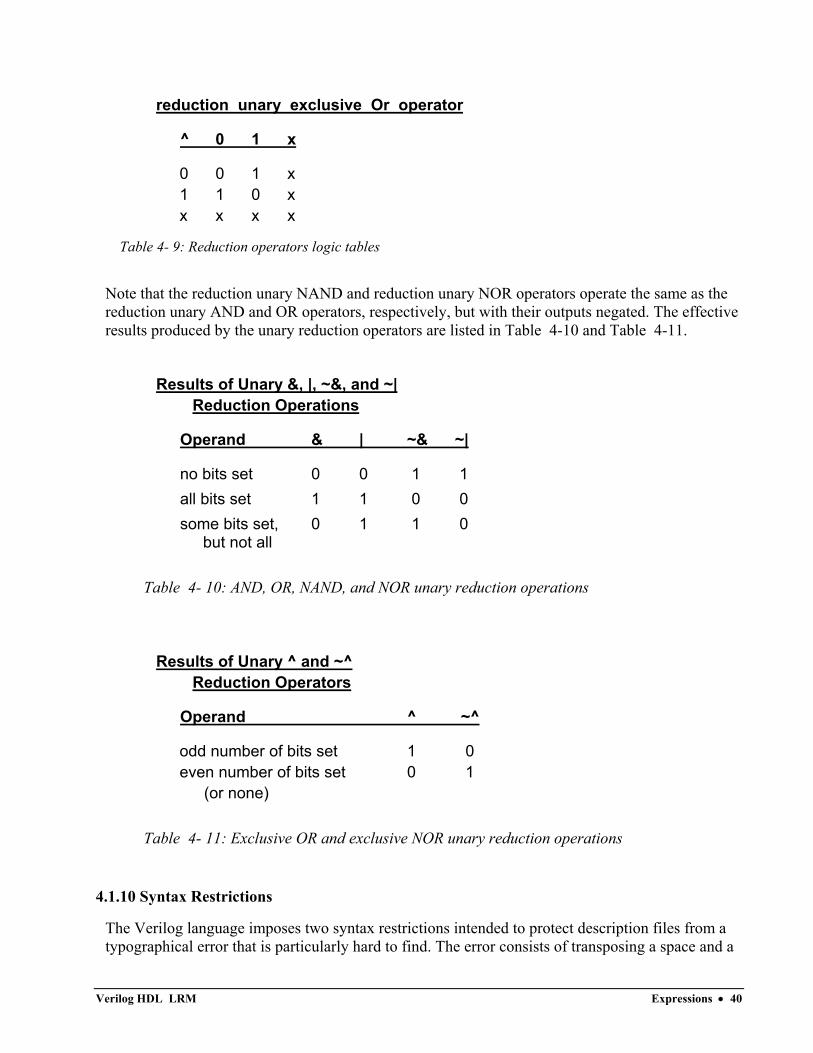
reduction unary exclusive Or operator
^ 0 1 x
0 0 1 x 1 1 0 x x x x x
Table 4- 9: Reduction operators logic tables
Note that the reduction unary NAND and reduction unary NOR operators operate the same as the reduction unary AND and OR operators, respectively, but with their outputs negated. The effective results produced by the unary reduction operators are listed in Table 4-10 and Table 4-11.
Results of Unary &, |, ~&, and ~| Reduction Operations
Operand & | ~& ~|
no bits set 0 0 1 1 all bits set 1 1 0 0 some bits set, 0 1 1 0
but not all
Table 4- 10: AND, OR, NAND, and NOR unary reduction operations
Results of Unary ^ and ~^ Reduction Operators
Operand ^ ~^
odd number of bits set 1 0 even number of bits set 0 1
(or none)
Table 4- 11: Exclusive OR and exclusive NOR unary reduction operations
4.1.10 Syntax Restrictions
The Verilog language imposes two syntax restrictions intended to protect description files from a typographical error that is particularly hard to find. The error consists of transposing a space and a
Verilog HDL LRM Expressions • 40
symbol. Note that the constructs on line 1 below do not represent the same syntax as the similar constructs on line 2.
1. a & &b a | |b
2. a && b a || b
In order to protect users from this type of error, Verilog requires the use of parentheses to separate a reduction or or and operator from a bit-wise or or and operator. Table 4-12 shows the syntax that requires parentheses:
Invalid Equivalent Syntax Syntax
a & &b a & (&b) a | |b a | (|b)
Table 4- 12: Syntax equivalents for syntax restriction
4.1.11 Shift Operators
The shift operators, << and >>, perform left and right shifts of their left operand by the number of bit positions given by the right operand. Both shift operators fill the vacated bit positions with zeroes. Example 4-3 illustrates this concept.
module shift; reg [3:0] start, result; initial begin start = 1; // Start is set to 0001 result = (start << 2); // Result is set to 0100 end endmodule
Example 4- 3: Use of shift operator
In this example, the register result is assigned the binary value 0100, which is 0001 shifted to the left two positions and zero filled.
4.1.12 Conditional Operator
The conditional operator has three operands separated by two operators in the following format:
Verilog HDL LRM Expressions • 41
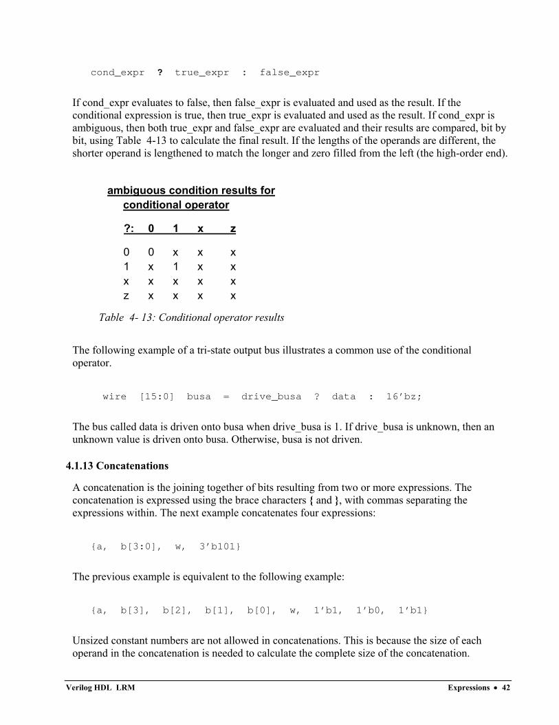
cond_expr ? true_expr : false_expr
If cond_expr evaluates to false, then false_expr is evaluated and used as the result. If the conditional expression is true, then true_expr is evaluated and used as the result. If cond_expr is ambiguous, then both true_expr and false_expr are evaluated and their results are compared, bit by bit, using Table 4-13 to calculate the final result. If the lengths of the operands are different, the shorter operand is lengthened to match the longer and zero filled from the left (the high-order end).
ambiguous condition results for conditional operator
?: 0 1 x z
0 0 x x x 1 x 1 x x x x x x x z x x x x
Table 4- 13: Conditional operator results
The following example of a tri-state output bus illustrates a common use of the conditional operator.
wire [15:0] busa = drive_busa ? data : 16’bz;
The bus called data is driven onto busa when drive_busa is 1. If drive_busa is unknown, then an unknown value is driven onto busa. Otherwise, busa is not driven.
4.1.13 Concatenations
A concatenation is the joining together of bits resulting from two or more expressions. The concatenation is expressed using the brace characters { and }, with commas separating the expressions within. The next example concatenates four expressions:
{a, b[3:0], w, 3’b101}
The previous example is equivalent to the following example:
{a, b[3], b[2], b[1], b[0], w, 1’b1, 1’b0, 1’b1}
Unsized constant numbers are not allowed in concatenations. This is because the size of each operand in the concatenation is needed to calculate the complete size of the concatenation.
Verilog HDL LRM Expressions • 42
Concatenations can be expressed using a repetition multiplier as shown in the next example.
{4{w}} // This is equivalent to {w, w, w, w}
The next example illustrates nested concatenations.
{b, {3{a, b}}} // This is equivalent to
// {b, a, b, a, b, a, b}
The repetition multiplier must be a constant expression.
4.2 Operands
As stated before, there are several types of operands that can be specified in expressions. The simplest type is a reference to a net or register in its complete form—that is, just the name of the net or register is given. In this case, all of the bits making up the net or register value are used as the operand.
If just a single bit of a vector net or register is required, then a bit-select operand is used. A part-select operand is used to reference a group of adjacent bits in a vector net or register.
A memory element can be referenced as an operand.
A concatenation of other operands, (including nested concatenations) can be specified as an operand.
A function call is an operand.
4.2.1 Net and Register Bit Addressing
Bit-selects extract a particular bit from a vector net or register. The bit can be addressed using an expression. The next example specifies the single bit of acc that is addressed by the operand index.
acc[index]
The actual bit that is accessed by an address is, in part, determined by the declaration of acc. For instance, each of the declarations of acc shown in the next example causes a particular value of index to access a different bit:
reg [15:0] acc;
reg [1:16] acc;
If the bit select is out of the address bounds or is x, then the value returned by the reference is x.
Verilog HDL LRM Expressions • 43
Several contiguous bits in a vector register or net can be addressed, and are known as part-selects. A part-select of a vector register or net is given with the following syntax:
vect[ms_expr:ls_expr]
Both expressions must be constant expressions. The first expression must address a more significant bit than the second expression. The next example and the bullet items that follow it illustrate the principles of bit addressing. The code declares an 8-bit register called vect and initializes it to a value of 4. The bullet items describe how the separate bits of that vector can be addressed.
reg [7:0] vect;
vect = 4;
• if the value of addr is 2, then vect[addr] returns 1
• if the value of addr is out of bounds, then vect[addr] returns x
• if addr is 0, 1, or 3 through 7, vect[addr] returns 0
• vect[3:0] returns the bits 0100
• vect[5:1] returns the bits 00010
• vect[<expression that returns x>] returns x
• vect[<expression that returns z>] returns x
• if any bit of addr is x/z, then the value of addr is x
4.2.2 Memory Addressing
Section 3.8 discussed the declaration of memories. This section discusses memory addressing. The next example declares a memory of 1024 8-bit words:
reg [7:0] mem_name[0:1023];
The syntax for a memory address consists of the name of the memory and an expression for the address—specified with the following format:
mem_name[addr_expr]
The addr_expr can be any expression; therefore, memory indirections can be specified in a single expression. The next example illustrates memory indirection:
Verilog HDL LRM Expressions • 44
mem_name[mem_name[3]]
In the above example, mem_name[3]addresses word three of the memory called mem_name. The value at word three is the index into mem_name that is used by the memory address mem_name[mem_name[3]]. As with bit-selects, the address bounds given in the declaration of the memory determine the effect of the address expression. If the index is out of the address bounds or is x, then the value of the reference is x.
There is no mechanism to express bit-selects or part-selects of memory elements directly. If this is required, then the memory element has to be first transferred to an appropriately sized temporary register.
4.2.3 Strings
String operands are treated as constant numbers consisting of a sequence of 8-bit ASCII codes, one per character.
Any Verilog HDL operator can manipulate string operands. The operator behaves as though the entire string were a single numeric value.
Example 4-4 declares a string variable large enough to hold 14 characters and assigns a value to it. The example then manipulates the string using the concatenation operator.
Note that when a variable is larger than required to hold the value being assigned, the contents after the assignment are padded on the left with zeros. This is consistent with the padding that occurs during assignment of non-string values.
module string_test; reg [8*14:1] stringvar; initial
begin stringvar = "Hello world"; $display("%s is stored as %h", stringvar, stringvar); stringvar={stringvar, "!!!"}; $display("%s is stored as %h", stringvar, stringvar); end
endmodule
Example 4- 4: Concatenation of strings
The result of running Verilog on the above description is:
Hello world is stored as 00000048656c6c6f20776f726c64
Hello world!!! is stored as 48656c6c6f20776f726c64212121
Verilog HDL LRM Expressions • 45
4.2.4 String Operations
The common string operations copy, concatenate, and compare are supported by Verilog operators. Copy is provided by simple assignment. Concatenation is provided by the concatenation operator. Comparison is provided by the equality operators. Example 4-4 and Example 4-5 illustrate assignment, concatenation, and comparison of strings.
When manipulating string values in vector variables, at least 8*n bits are required in the vector, where n is the number of characters in the string.
4.2.5 String Value Padding and Potential Problems
When strings are assigned to variables, the values stored are padded on the left with zeros. Padding can affect the results of comparison and concatenation operations. The comparison and concatenation operators do not distinguish between zeros resulting from padding and the original string characters.
Example 4-5 illustrates the potential problem.
reg [8*10:1] s1, s2; initial begin s1 = "Hello"; s2 = "world!"; if ( {s1,s2} == "Hello world!") $display("strings are equal"); end
Example 4- 5: Comparing string variables
The comparison in the example above fails because during the assignment the string variables get padded as illustrated in the next example:
s1 = 000000000048656c6c6f
s2 = 00000020776f726c6421
The concatenation of s1 and s2 includes the zero padding, resulting in the following value:
000000000048656c6c6f00000020776f726c6421
Since the string “Hello world” contains no zero padding, the comparison fails, as shown below: s1 s2 "Hello world!"
000000000048656c6c6f 00000020776f726c6421 == 48656c6c6f20776f726c6421 "Hello" "world!"
Verilog HDL LRM Expressions • 46
The above comparison yields a result of zero, which is equivalent to false.
4.2.6 Null String Handling
The null string ("") is equivalent to the value zero (0).
4.3 Minimum, Typical, Maximum Delay Expressions
Verilog HDL delay expressions can be specified as three expressions separated by colons. This triple is intended to represent minimum, typical, and maximum values—in that order. The syntax is as follows:
<mintypmax_expression> ::= <expression> ||= <expression1> : <expression2> : <expression3>
Syntax 4- 1: Syntax for <mintypmax_expression>
The three expressions follow these conventions:
• expression1 is less than or equal to expression2
• expression2 is less than or equal to expression3
Verilog models typically specify three values for delay expressions. The three values allow a design to be tested with minimum, typical, or maximum delay values. Different tools may interpret the triple form of an expression in a different manner. In the following example, one of the three specified delays will be executed before the simulation executes the assignment; if the user does not select one, the simulator will take the default.
always @A
X = #(3:4:5) A;
Values expressed in min:typ:max format can be used in expressions. The next example shows an expression that defines a single triplet of delay values. The minimum value is the sum of a+d; the typical value is b+e; the maximum value is c+f, as follows:
(a:b:c) + (d:e:f)
The next example shows some typical expressions that are used to specify min:typ:max format values:
val - (32’d 50: 32’d 75: 32’d 100)
Verilog HDL LRM Expressions • 47
The min:typ:max format can be used wherever expressions can appear, both in source text files and in interactive commands. See also 6.15.1 min/typ/max Delays
4.4 Expression Bit Lengths
Controlling the number of bits that are used in expression evaluations is important if consistent results are to be achieved. Some situations have a simple solution, for example, if a bit-wise AND operation is specified on two 16-bit registers, then the result is a 16-bit value. However, in some situations it is not obvious how many bits are used to evaluate an expression, what size the result should be, or whether signed or unsigned arithmetic should be used.
For example, when is it necessary to perform the addition of two 16-bit registers in 17 bits to handle a possible carry overflow? The answer depends on the context in which the addition takes place. If the 16-bit addition is modeling a real 16-bit adder that loses or does not care about the carry overflow, then the model must perform the addition in 16 bits. If the addition of two 16-bit unsigned numbers can result in a significant 17th bit, then assign the answer to a 17-bit register.
4.4.1 An Example of an Expression Bit Length Problem
During the evaluation of an expression, interim results take the size of the largest operand (in the case of an assignment, this also includes the left-hand side). You must therefore take care to prevent loss of a significant bit during expression evaluation. This section describes an example of the problems that can occur.
The expression (a + b >> 1) yields a 16-bit result, but cannot be assigned to a 16-bit register without the potential loss of the high-order bit. If a and b are 16-bit registers, then the result of (a+b) is 16 bits wide—unless the result is assigned to a register wider than 16 bits. If answer is a 17-bit register, then (answer = a + b) yields a full 17-bit result. But in the expression (a + b >> 1), the sum of (a + b) produces an interim result that is only 16 bits wide. Therefore, the assignment of (a + b >> 1) to a 16-bit register loses the carry bit before the evaluation performs the one-bit right shift.
There are two solutions to a problem of this type. One is to assign the sum of (a+b) to a 17-bit register before performing the shift and then shift the 17-bit answer into the 16-bits that your model requires. An easier solution is to use the following trick:
The problem:
Evaluate the expression (a+b)>>1, assigning the result to a 16-bit register without losing the carry bit. Variables a and b are both 16-bit registers.
The solution:
Add the integer zero to the expression. The expression evaluates as follows:
1. 0 + (a+b) evaluates—the result is as wide as the widest term, which is the 32-bit zero
2. the 32-bit sum of 0 + (a+b) is shifted right one bit This trick preserves the carry bit until the shift operation can move it back down into 16 bits.
Verilog HDL LRM Expressions • 48
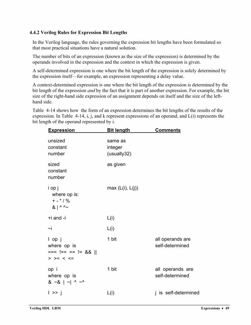
4.4.2 Verilog Rules for Expression Bit Lengths
In the Verilog language, the rules governing the expression bit lengths have been formulated so that most practical situations have a natural solution.
The number of bits of an expression (known as the size of the expression) is determined by the operands involved in the expression and the context in which the expression is given.
A self-determined expression is one where the bit length of the expression is solely determined by the expression itself—for example, an expression representing a delay value.
A context-determined expression is one where the bit length of the expression is determined by the bit length of the expression and by the fact that it is part of another expression. For example, the bit size of the right-hand side expression of an assignment depends on itself and the size of the left-hand side.
Table 4-14 shows how the form of an expression determines the bit lengths of the results of the expression. In Table 4-14, i, j, and k represent expressions of an operand, and L(i) represents the bit length of the operand represented by i.
Expression Bit length Comments
unsized same as constant integer number (usually32)
sized as given constant number
i op j max (L(i), L(j)) where op is: + - * / % & | ^ ^~
+i and -i L(i)
~i L(i)
I op j 1 bit all operands are where op is self-determined === !== == != && || > >= < <=
op i 1 bit all operands are where op is self-determined & ~& | ~| ^ ~^
I >> j L(i) j is self-determined
Verilog HDL LRM Expressions • 49
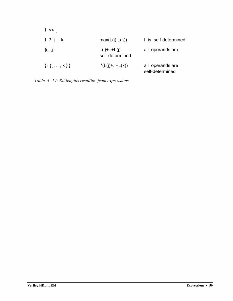
I << j
I ? j : k max(L(j),L(k)) I is self-determined
{i,..,j} L(i)+..+L(j) all operands are self-determined
{ i { j, .. , k } } i*(L(j)+..+L(k)) all operands are self-determined
Table 4- 14: Bit lengths resulting from expressions
Verilog HDL LRM Expressions • 50
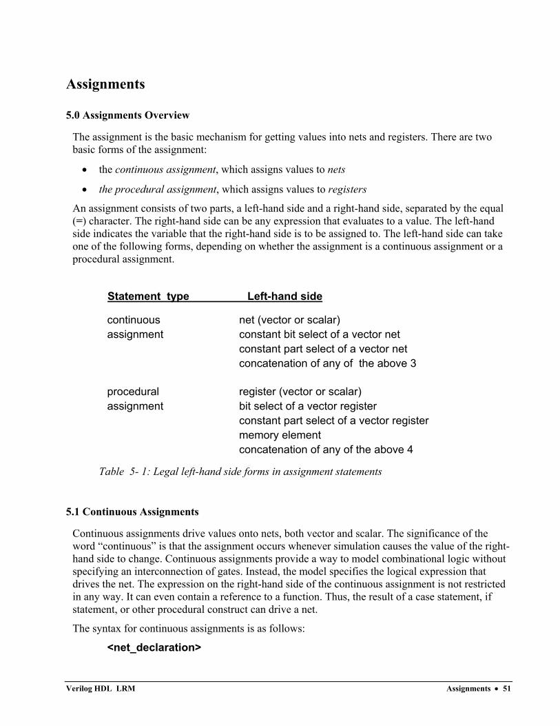
Assignments
5.0 Assignments Overview
The assignment is the basic mechanism for getting values into nets and registers. There are two basic forms of the assignment:
• the continuous assignment, which assigns values to nets
• the procedural assignment, which assigns values to registers
An assignment consists of two parts, a left-hand side and a right-hand side, separated by the equal (=) character. The right-hand side can be any expression that evaluates to a value. The left-hand side indicates the variable that the right-hand side is to be assigned to. The left-hand side can take one of the following forms, depending on whether the assignment is a continuous assignment or a procedural assignment.
Statement type Left-hand side
continuous net (vector or scalar) assignment constant bit select of a vector net constant part select of a vector net concatenation of any of the above 3
procedural register (vector or scalar) assignment bit select of a vector register constant part select of a vector register memory element concatenation of any of the above 4
Table 5- 1: Legal left-hand side forms in assignment statements
5.1 Continuous Assignments
Continuous assignments drive values onto nets, both vector and scalar. The significance of the word “continuous” is that the assignment occurs whenever simulation causes the value of the right-hand side to change. Continuous assignments provide a way to model combinational logic without specifying an interconnection of gates. Instead, the model specifies the logical expression that drives the net. The expression on the right-hand side of the continuous assignment is not restricted in any way. It can even contain a reference to a function. Thus, the result of a case statement, if statement, or other procedural construct can drive a net.
The syntax for continuous assignments is as follows:
<net_declaration>
Verilog HDL LRM Assignments • 51
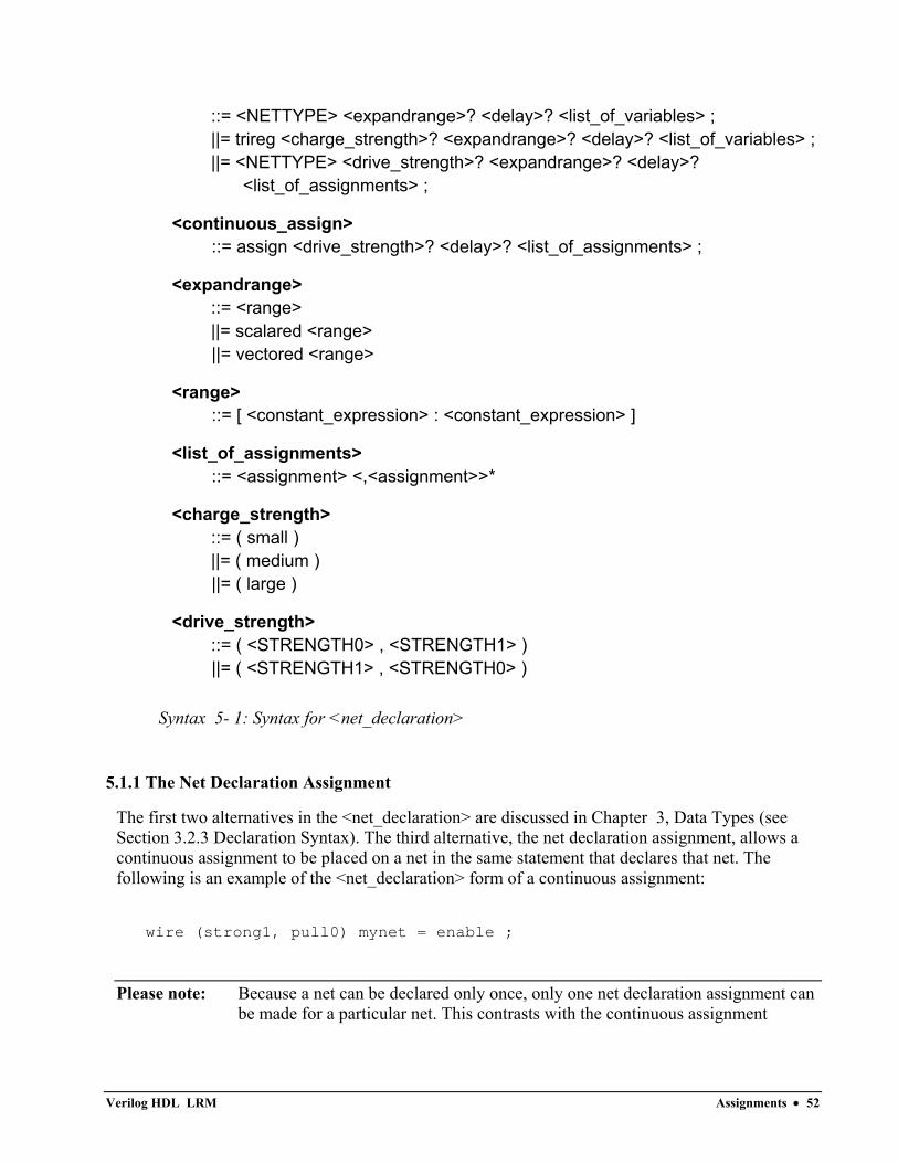
::= <NETTYPE> <expandrange>? <delay>? <list_of_variables> ; ||= trireg <charge_strength>? <expandrange>? <delay>? <list_of_variables> ; ||= <NETTYPE> <drive_strength>? <expandrange>? <delay>?
<list_of_assignments> ;
<continuous_assign> ::= assign <drive_strength>? <delay>? <list_of_assignments> ;
<expandrange> ::= <range> ||= scalared <range> ||= vectored <range>
<range> ::= [ <constant_expression> : <constant_expression> ]
<list_of_assignments> ::= <assignment> <,<assignment>>*
<charge_strength> ::= ( small ) ||= ( medium ) ||= ( large )
<drive_strength> ::= ( <STRENGTH0> , <STRENGTH1> ) ||= ( <STRENGTH1> , <STRENGTH0> )
Syntax 5- 1: Syntax for <net_declaration>
5.1.1 The Net Declaration Assignment
The first two alternatives in the <net_declaration> are discussed in Chapter 3, Data Types (see Section 3.2.3 Declaration Syntax). The third alternative, the net declaration assignment, allows a continuous assignment to be placed on a net in the same statement that declares that net. The following is an example of the <net_declaration> form of a continuous assignment:
wire (strong1, pull0) mynet = enable ;
Please note: Because a net can be declared only once, only one net declaration assignment can be made for a particular net. This contrasts with the continuous assignment
Verilog HDL LRM Assignments • 52
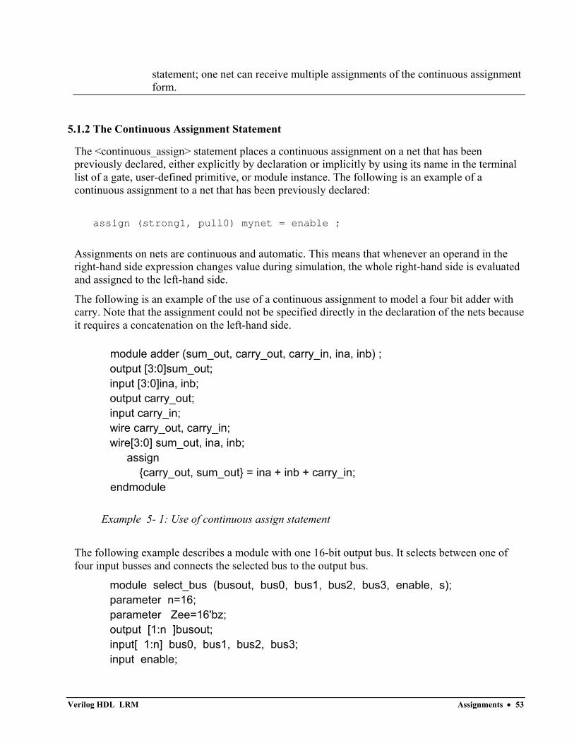
statement; one net can receive multiple assignments of the continuous assignment form.
5.1.2 The Continuous Assignment Statement
The <continuous_assign> statement places a continuous assignment on a net that has been previously declared, either explicitly by declaration or implicitly by using its name in the terminal list of a gate, user-defined primitive, or module instance. The following is an example of a continuous assignment to a net that has been previously declared:
assign (strong1, pull0) mynet = enable ;
Assignments on nets are continuous and automatic. This means that whenever an operand in the right-hand side expression changes value during simulation, the whole right-hand side is evaluated and assigned to the left-hand side.
The following is an example of the use of a continuous assignment to model a four bit adder with carry. Note that the assignment could not be specified directly in the declaration of the nets because it requires a concatenation on the left-hand side.
module adder (sum_out, carry_out, carry_in, ina, inb) ; output [3:0]sum_out; input [3:0]ina, inb; output carry_out; input carry_in; wire carry_out, carry_in; wire[3:0] sum_out, ina, inb; assign {carry_out, sum_out} = ina + inb + carry_in; endmodule
Example 5- 1: Use of continuous assign statement
The following example describes a module with one 16-bit output bus. It selects between one of four input busses and connects the selected bus to the output bus.
module select_bus (busout, bus0, bus1, bus2, bus3, enable, s); parameter n=16; parameter Zee=16'bz; output [1:n ]busout; input[ 1:n] bus0, bus1, bus2, bus3; input enable;
Verilog HDL LRM Assignments • 53
input 1:2] s; tri [1:n] data; // net declaration. tri [1:n] busou t= enable ? data : Zee; // net declaration with // continuous assignment. assign // assignment statement with
data = (s==0) ? bus0 : Zee, // 4 continuous assignments. data = (s==1) ? bus1 : Zee, data = (s==2) ? bus2 : Zee, data = (s==3) ? bus3 : Zee;
endmodule
Example 5- 2: Net declaration assignment and continuous assign statement
The following sequence of events is experienced during simulation of the description in Example 5-2:
1. The value of s, a bus selector input variable, is checked in the assign statement; based on the value of s, the net data receives the data from one of the four input busses.
2. The setting of data triggers the continuous assignment in the net declaration for busout; if enable is set, the contents of data are assigned to busout; if enable is clear, the contents of Zee are assigned to busout.
5.1.3 Delays
A delay given to a continuous assignment specifies the time duration between a right-hand side operand value change and the assignment made to the left-hand side. If the left-hand side references a scalar net, then the delay is treated in the same way as for gate delays—that is, different delays can be given for the output rising, falling and changing to high impedance (see Chapter 6, 6.15 Gate and Net Delays).
If the left-hand side references a vector net, then up to three delays can also be applied. The following rules determine which delay controls the assignment:
• If the right-hand side was non-zero and becomes zero, then the falling delay is used.
• If the right-hand side becomes z, then the turn-off delay is used.
• For other cases, the rising delay is used.
Note that specifying the delay in a continuous assignment that is part of the net declaration is different from specifying a net delay and then making a continuous assignment to the net. A delay value can be applied to a net in a net declaration, as in the following example:
wire #10 wireA;
Verilog HDL LRM Assignments • 54
This syntax, called a net delay, means that any value change that is to be applied to wireA by some other statement is delayed for ten time units before it takes effect. When there is a continuous assignment in a declaration, the delay is part of the continuous assignment and is not a net delay. Thus, it is not added to the delay of other drivers on the net. Furthermore, if the assignment is to an expanded vector net (a net not specified with the keyword vectored), then the rising and falling delays are not applied to the individual bits if the assignment is included in the declaration.
In situations where a right-hand side operand changes before a previous change has had time to propagate to the left-hand side, then the latest value change is the only one to be applied. That is, only one assignment occurs. This effect is known as inertial delay.
The following example implements a vector exclusive OR. The size and delay of the operation are controlled by parameters, which can be changed when instances of this module are created. See Section 12.2 Overriding Module Parameter Values for details on overriding parameter values.
module modxor (axorb, a, b); parameter size=8, delay=15; output [size-1:0] axorb; input [size-1:0] a, b; wire [size-1:0] #delay axorb = a ^ b; endmodule
Example 5- 3: Use of delays with assignments
5.1.4 Strength
The driving strength of a continuous assignment can be specified by the user. This applies only to assignments to scalar nets of the types listed below:
wire wand tri trireg
wor triand tri0
trior tri1
Continuous assignments driving strengths can be specified in either a net declaration or in a stand-alone assignment, using the assign keyword. The strength specification, if provided, must immediately follow the keyword (either the keyword for the net type or the assign keyword) and must precede any delay specified. Whenever the continuous assignment drives the net, the strength of the value will simulate as specified.
A <drive_strength> specification contains one strength value that applies when the value being assigned to the net is 1 and a second strength value that applies when the assigned value is 0. The follow- ing keywords specify the strength value for an assignment of 1:
supply1 strong1 pull1 weak1 highz1
The following keywords specify the strength value for an assignment of 0:
Verilog HDL LRM Assignments • 55
supply0 strong0 pull0 weak0 highz0
The order of the two strength specifications is arbitrary. The following two rules constrain the use of drive strength specifications:
• The strength specifications (highz1, highz0) and (highz0, highz1) are illegal language constructs.
• When the keyword vectored is specified together with a specification of strength on a continuous assignment, the keyword vectored is ignored.
5.2 Procedural Assignments
The primary discussion of procedural assignments is in Section 8.2 Procedural Assignments and 11.1 The assign and deassign Procedural Statements. However, a description of the basic ideas here will highlight the differences between continuous assignments and procedural assignments.
As stated above, continuous assignments drive nets in a manner similar to the way gates drive nets. The expression on the right-hand side can be thought of as a combinatorial circuit that drives the net continuously. In contrast, procedural assignments put values in registers. The assignment does not have duration; instead, the register holds the value of the assignment until the next procedural assignment to that register.
Procedural assignments occur within procedures such as always, initial, task and function (these procedures are described in later chapters) and can be thought of as "triggered" assignments. The trigger occurs when the flow of execution in the simulation reaches an assignment within a procedure. Reaching the assignment can be controlled by conditional statements. Event controls, delay controls, if statements, case statements, and looping statements can all be used to control whether assignments get evaluated. Chapter 8, Behavioral Modeling, gives details and examples.
Verilog HDL LRM Assignments • 56
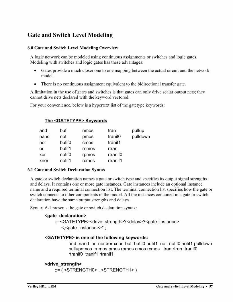
Gate and Switch Level Modeling
6.0 Gate and Switch Level Modeling Overview
A logic network can be modeled using continuous assignments or switches and logic gates. Modeling with switches and logic gates has these advantages:
• Gates provide a much closer one to one mapping between the actual circuit and the network model.
• There is no continuous assignment equivalent to the bidirectional transfer gate.
A limitation in the use of gates and switches is that gates can only drive scalar output nets; they cannot drive nets declared with the keyword vectored.
For your convenience, below is a hypertext list of the gatetype keywords:
The <GATETYPE> Keywords
and buf nmos tran pullup nand not pmos tranif0 pulldown nor bufif0 cmos tranif1 or bufif1 rnmos rtran xor notif0 rpmos rtranif0 xnor notif1 rcmos rtranif1
6.1 Gate and Switch Declaration Syntax
A gate or switch declaration names a gate or switch type and specifies its output signal strengths and delays. It contains one or more gate instances. Gate instances include an optional instance name and a required terminal connection list. The terminal connection list specifies how the gate or switch connects to other components in the model. All the instances contained in a gate or switch declaration have the same output strengths and delays.
Syntax 6-1 presents the gate or switch declaration syntax:
<gate_declaration> ::=<GATETYPE><drive_strength>?<delay>?<gate_instance> <,<gate_instance>>* ;
<GATETYPE> is one of the following keywords: and nand or nor xor xnor buf bufif0 bufif1 not notif0 notif1 pulldown
pullupnmos rnmos pmos rpmos cmos rcmos tran rtran tranif0 rtranif0 tranif1 rtranif1
<drive_strength> ::= ( <STRENGTH0> , <STRENGTH1> )
Verilog HDL LRM Gate and Switch Level Modeling • 57
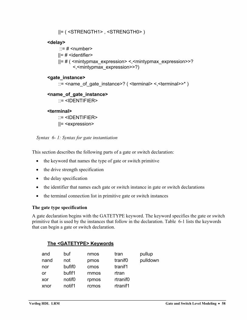
||= ( <STRENGTH1> , <STRENGTH0> )
<delay> ::= # <number> ||= # <identifier> ||= # ( <mintypmax_expression> <,<mintypmax_expression>>?
<,<mintypmax_expression>>?)
<gate_instance> ::= <name_of_gate_instance>? ( <terminal> <,<terminal>>* )
<name_of_gate_instance> ::= <IDENTIFIER>
<terminal> ::= <IDENTIFIER> ||= <expression>
Syntax 6- 1: Syntax for gate instantiation
This section describes the following parts of a gate or switch declaration:
• the keyword that names the type of gate or switch primitive
• the drive strength specification
• the delay specification
• the identifier that names each gate or switch instance in gate or switch declarations
• the terminal connection list in primitive gate or switch instances
The gate type specification
A gate declaration begins with the GATETYPE keyword. The keyword specifies the gate or switch primitive that is used by the instances that follow in the declaration. Table 6-1 lists the keywords that can begin a gate or switch declaration.
The <GATETYPE> Keywords
and buf nmos tran pullup nand not pmos tranif0 pulldown nor bufif0 cmos tranif1 or bufif1 rnmos rtran xor notif0 rpmos rtranif0 xnor notif1 rcmos rtranif1
Verilog HDL LRM Gate and Switch Level Modeling • 58
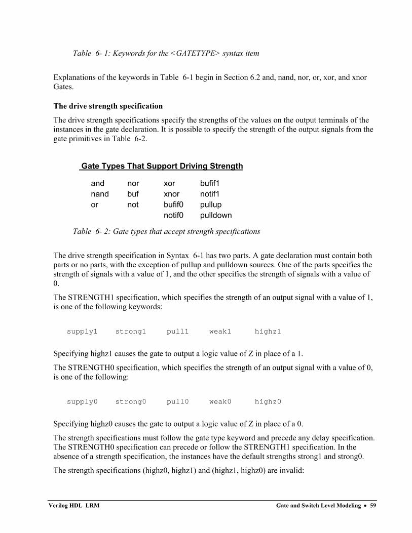
Table 6- 1: Keywords for the <GATETYPE> syntax item
Explanations of the keywords in Table 6-1 begin in Section 6.2 and, nand, nor, or, xor, and xnor Gates.
The drive strength specification
The drive strength specifications specify the strengths of the values on the output terminals of the instances in the gate declaration. It is possible to specify the strength of the output signals from the gate primitives in Table 6-2.
Gate Types That Support Driving Strength
and nor xor bufif1 nand buf xnor notif1 or not bufif0 pullup notif0 pulldown
Table 6- 2: Gate types that accept strength specifications
The drive strength specification in Syntax 6-1 has two parts. A gate declaration must contain both parts or no parts, with the exception of pullup and pulldown sources. One of the parts specifies the strength of signals with a value of 1, and the other specifies the strength of signals with a value of 0.
The STRENGTH1 specification, which specifies the strength of an output signal with a value of 1, is one of the following keywords:
supply1 strong1 pull1 weak1 highz1
Specifying highz1 causes the gate to output a logic value of Z in place of a 1.
The STRENGTH0 specification, which specifies the strength of an output signal with a value of 0, is one of the following:
supply0 strong0 pull0 weak0 highz0
Specifying highz0 causes the gate to output a logic value of Z in place of a 0.
The strength specifications must follow the gate type keyword and precede any delay specification. The STRENGTH0 specification can precede or follow the STRENGTH1 specification. In the absence of a strength specification, the instances have the default strengths strong1 and strong0.
The strength specifications (highz0, highz1) and (highz1, highz0) are invalid:
Verilog HDL LRM Gate and Switch Level Modeling • 59
The following example shows a drive strength specification in a declaration of an open collector nor gate:
nor(highz1,strong0)(out1,in1,in2);
In this example, the nor gate outputs a Z in place of a 1.
Sections 6.10 Logic Strength Modeling through 6.12 Strength Reduction by Non-Resistive Devices discuss logic strength modeling in more detail.
The delay specification
The delay specifies the propagation delay through the gates and switches in a declaration. Gates and switches in declarations with no delay specification have no propagation delay. A delay specification can contain up to three delay values, depending on its gate type. Section 6.2 and, nand, nor, or, xor, and xnor Gates begins discussions of each type of gate that detail the applicable delays. Section 6.15 Gate and Net Delays discusses delays in more detail. pullup and pulldown source declarations do not include delay specifications.
The primitive instance identifier
The IDENTIFIER in Syntax 6-1 is an optional name given to a gate or switch instance. The name is useful in tracing the operation of the circuit during debugging.
Primitive instance connection list
The <terminal>s at the end of Syntax 6-1 are the terminal list. The terminal list describes how the gate or switch connects to the rest of the model. The gate or switch type limits these expressions. The output or bidirectional terminals always come first in the terminal list, followed by the input terminals.
6.2 and, nand, nor, or, xor, and xnor Gates
Declarations of these gates begin with one of these keywords:
and nand nor or xor xnor
The delay specification can be zero, one, or two delays. If there is no delay, there is no delay through the gate. One delay specifies the delays for all output transitions. If the specification contains two delays, the first delay determines the rise delay, the second delay determines the fall delay, and the smaller of the two delays applies to transitions to X and Z.
These six gates have one output and one or more inputs. The first terminal in the terminal list connects to the gate’s output and all other terminals connect to its inputs.
The truth tables for these gates, showing the result of two input values, appear in Table 6-3.
Verilog HDL LRM Gate and Switch Level Modeling • 60
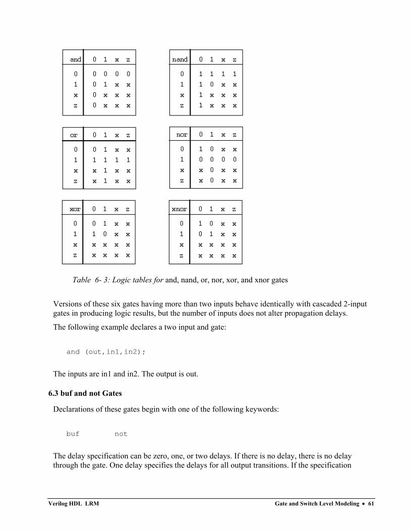
Table 6- 3: Logic tables for and, nand, or, nor, xor, and xnor gates
Versions of these six gates having more than two inputs behave identically with cascaded 2-input gates in producing logic results, but the number of inputs does not alter propagation delays.
The following example declares a two input and gate:
and (out,in1,in2);
The inputs are in1 and in2. The output is out.
6.3 buf and not Gates
Declarations of these gates begin with one of the following keywords:
buf not
The delay specification can be zero, one, or two delays. If there is no delay, there is no delay through the gate. One delay specifies the delays for all output transitions. If the specification
Verilog HDL LRM Gate and Switch Level Modeling • 61
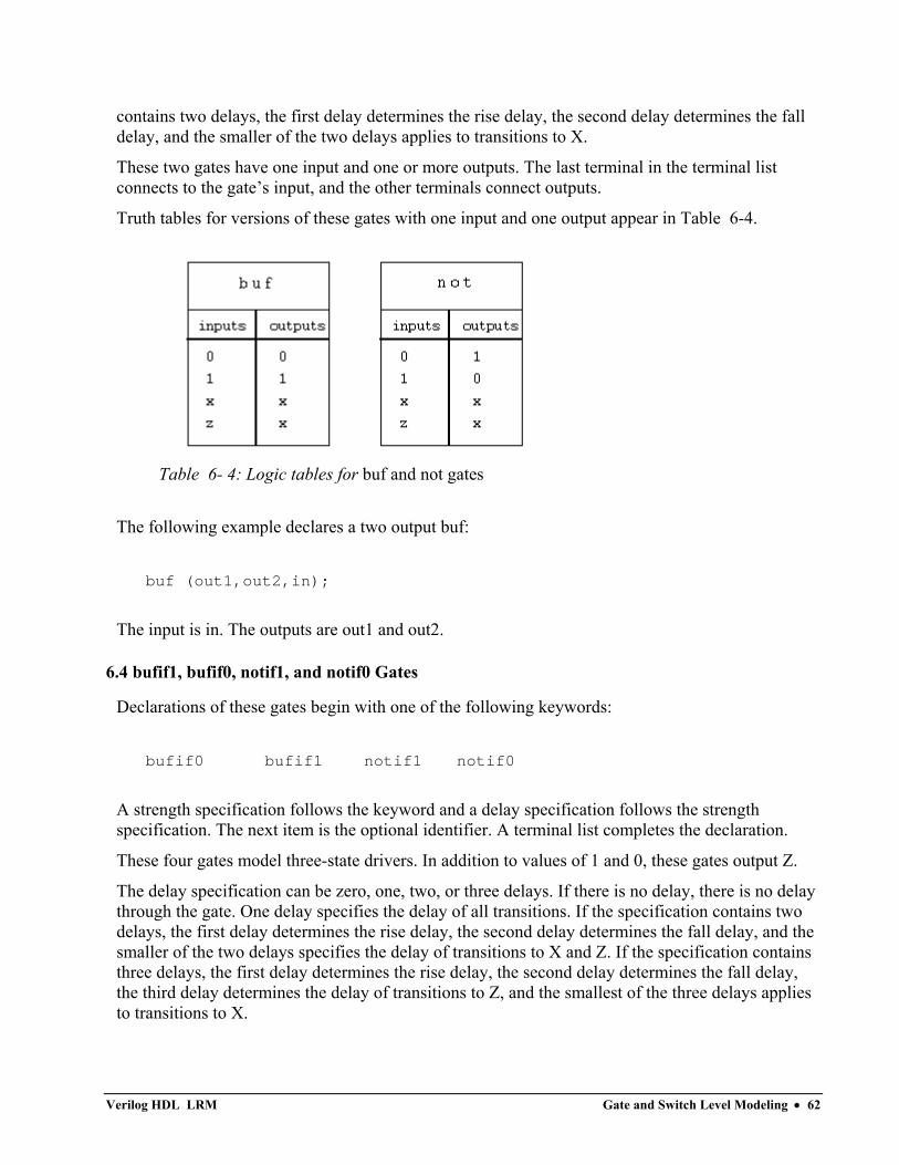
contains two delays, the first delay determines the rise delay, the second delay determines the fall delay, and the smaller of the two delays applies to transitions to X.
These two gates have one input and one or more outputs. The last terminal in the terminal list connects to the gate’s input, and the other terminals connect outputs.
Truth tables for versions of these gates with one input and one output appear in Table 6-4.
Table 6- 4: Logic tables for buf and not gates
The following example declares a two output buf:
buf (out1,out2,in);
The input is in. The outputs are out1 and out2.
6.4 bufif1, bufif0, notif1, and notif0 Gates
Declarations of these gates begin with one of the following keywords:
bufif0 bufif1 notif1 notif0
A strength specification follows the keyword and a delay specification follows the strength specification. The next item is the optional identifier. A terminal list completes the declaration.
These four gates model three-state drivers. In addition to values of 1 and 0, these gates output Z.
The delay specification can be zero, one, two, or three delays. If there is no delay, there is no delay through the gate. One delay specifies the delay of all transitions. If the specification contains two delays, the first delay determines the rise delay, the second delay determines the fall delay, and the smaller of the two delays specifies the delay of transitions to X and Z. If the specification contains three delays, the first delay determines the rise delay, the second delay determines the fall delay, the third delay determines the delay of transitions to Z, and the smallest of the three delays applies to transitions to X.
Verilog HDL LRM Gate and Switch Level Modeling • 62
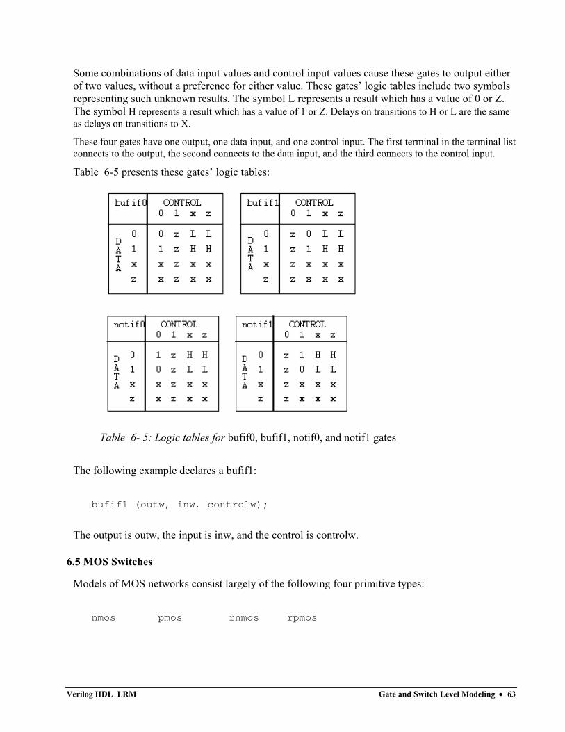
Some combinations of data input values and control input values cause these gates to output either of two values, without a preference for either value. These gates’ logic tables include two symbols representing such unknown results. The symbol L represents a result which has a value of 0 or Z. The symbol H represents a result which has a value of 1 or Z. Delays on transitions to H or L are the same as delays on transitions to X.
These four gates have one output, one data input, and one control input. The first terminal in the terminal list connects to the output, the second connects to the data input, and the third connects to the control input.
Table 6-5 presents these gates’ logic tables:
Table 6- 5: Logic tables for bufif0, bufif1, notif0, and notif1 gates
The following example declares a bufif1:
bufif1 (outw, inw, controlw);
The output is outw, the input is inw, and the control is controlw.
6.5 MOS Switches
Models of MOS networks consist largely of the following four primitive types:
nmos pmos rnmos rpmos
Verilog HDL LRM Gate and Switch Level Modeling • 63
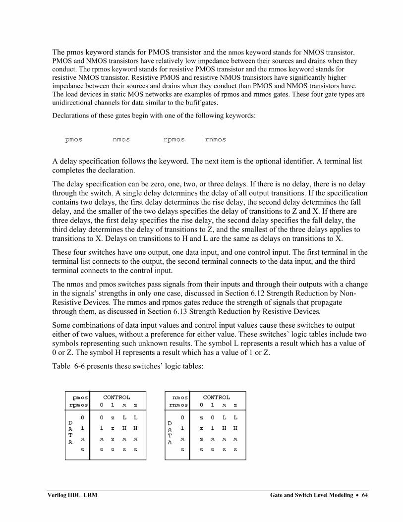
The pmos keyword stands for PMOS transistor and the nmos keyword stands for NMOS transistor. PMOS and NMOS transistors have relatively low impedance between their sources and drains when they conduct. The rpmos keyword stands for resistive PMOS transistor and the rnmos keyword stands for resistive NMOS transistor. Resistive PMOS and resistive NMOS transistors have significantly higher impedance between their sources and drains when they conduct than PMOS and NMOS transistors have. The load devices in static MOS networks are examples of rpmos and rnmos gates. These four gate types are unidirectional channels for data similar to the bufif gates.
Declarations of these gates begin with one of the following keywords:
pmos nmos rpmos rnmos
A delay specification follows the keyword. The next item is the optional identifier. A terminal list completes the declaration.
The delay specification can be zero, one, two, or three delays. If there is no delay, there is no delay through the switch. A single delay determines the delay of all output transitions. If the specification contains two delays, the first delay determines the rise delay, the second delay determines the fall delay, and the smaller of the two delays specifies the delay of transitions to Z and X. If there are three delays, the first delay specifies the rise delay, the second delay specifies the fall delay, the third delay determines the delay of transitions to Z, and the smallest of the three delays applies to transitions to X. Delays on transitions to H and L are the same as delays on transitions to X.
These four switches have one output, one data input, and one control input. The first terminal in the terminal list connects to the output, the second terminal connects to the data input, and the third terminal connects to the control input.
The nmos and pmos switches pass signals from their inputs and through their outputs with a change in the signals’ strengths in only one case, discussed in Section 6.12 Strength Reduction by Non-Resistive Devices. The rnmos and rpmos gates reduce the strength of signals that propagate through them, as discussed in Section 6.13 Strength Reduction by Resistive Devices.
Some combinations of data input values and control input values cause these switches to output either of two values, without a preference for either value. These switches’ logic tables include two symbols representing such unknown results. The symbol L represents a result which has a value of 0 or Z. The symbol H represents a result which has a value of 1 or Z.
Table 6-6 presents these switches’ logic tables:
Verilog HDL LRM Gate and Switch Level Modeling • 64
Table 6- 6: Logic tables for pmos, rpmos, nmos, and rnmos gates
The following example declares a pmos switch:
pmos (out,data,control);
The output is out, the data input is data, and the control input is control.
6.6 Bidirectional Pass Switches
Declarations of these devices begin with one of the following keywords:
tran tranif1 tranif0
rtran rtranif1 rtranif0
A delay specification follows the keywords in declarations of tranif1, tranif0, rtranif1, and rtranif0; the tran and rtran devices do not take delays. The next item is the optional identifier. A terminal list completes the declaration.
The delay specifications for tranif1, tranif0, rtranif1, and rtranif0 devices can be zero, one, or two delays. If there is no delay, the device has no turn-on or turn-off delay. If the specification contains one delay, that delay determines both turn-on and turn-off delays. If there are two delays, the first delay specifies the turn-on delay, and the second delay specifies the turn-off delay.
These six devices do not delay signals propagating through them. When these devices are turned off they block signals, and when they are turned on they pass signals.
The tranif1, tranif0, rtranif1, and rtranif0 devices have three items in their terminal lists. Two are bidirectional terminals that conduct signals to and from the devices, and the other terminal connects to a control input. The terminals connected to inouts precede the terminal connected to the control input in the terminal list.
The tran and rtran devices have terminal lists containing two bidirectional terminals.
The bidirectional terminals of all six of these devices connect only to scalar nets or bit selects of expanded vector nets.
The tran, tranif0, and rtranif1 devices pass signals with an alteration in their strength in only one case, discussed in Section 6.12 Strength Reduction by Non-Resistive Devices. The rtran, rtranif0, and rtranif1 devices reduce the strength of signals passing through them according to rules discussed in Section 6.13 Strength Reduction by Resistive Devices.
The following example declares a tranif1:
tranif1 (inout1,inout2,control);
Verilog HDL LRM Gate and Switch Level Modeling • 65
The bidirectional terminals are inout1 and inout2. The control input is control.
6.7 cmos Gates
Declarations of these gates begins with one of these keywords:
cmos rcmos
The delay specification can be zero, one, two, or three delays. If there is no delay, there is no delay through the gate. A single delay specifies the delay for all transitions. If the specification contains two delays, the first delay determines the rise delay, the second delay determines the fall delay, and the smaller of the two delays is the delay of transitions to Z and X. If the specification contains three delays, the first delay controls rise delays, the second delay controls fall delays, the third delay controls transitions to Z, and the smallest of the three delays applies to transitions to X. Delays in transitions to H or L are the same as delays in transitions to X.
The cmos and rcmos gates have a data input, a data output, and two control inputs. In the terminal list, the first terminal connects to the data output, the second connects to the data input, the third connects to the n-channel control input, and the last connects to the p-channel control input.
The cmos gate passes signals with an alteration in their strength in only one case, discussed in subsection 6.12 Strength Reduction by Non-Resistive Devices. The rcmos gate reduces the strength of signals passing through it according to rules that appear in Section 6.13 Strength Reduction by Resistive Devices.
The cmos gate is the combination of a pmos gate and an nmos gate. The rcmos gate is the combination of an rpmos gate and an rnmos gate. The combined gates in these configurations share data input and data output terminals, but they have separate control inputs.
The equivalence of the cmos gate to the pairing of an nmos gate and a pmos gate is detailed in the following explanation:
cmos (w, datain, ncontrol, pcontrol);
is equivalent to:
nmos (w, datain, ncontrol);
pmos (w, datain, pcontrol);
6.8 pullup and pulldown Sources
Declarations of these sources begin with one of the following keywords:
pullup pulldown
Verilog HDL LRM Gate and Switch Level Modeling • 66
A strength specification follows the keyword, and an optional identifier follows the strength specification. A terminal list completes the declaration.
A pullup source places a logic value of 1 on the nets listed in its terminal list. A pulldown source places a logic value of 0 on the nets listed in its terminal list. The signals that these sources place on nets have pull strength in the absence of a strength specification. There are no delay specifications for these sources because the signals they place on nets continue throughout simulation without variation.
The following example declares two pullup instances:
pullup (strong1)(neta),(netb);
In this example, one gate instance drives neta and the other drives netb.
6.9 Implicit Net Declarations
Including a previously unused identifier in a terminal list implicitly declares a new net of the wire type with zero delay.
Each implicitly declared net must connect to one or more of the following:
• gate output
• tranif bidirectional terminal
• module output port
Refer to Section C.2 `default_nettype for a discussion of the compiler directive ‘default_nettype.
6.10 Logic Strength Modeling
The Verilog HDL provides for accurate modeling of signal contention, bidirectional pass gates, resistive MOS devices, dynamic MOS, charge sharing, and other technology dependent network configurations by allowing scalar net signal values to have a full range of unknown values and different levels of strength or combinations of levels of strength. This multiple level logic strength modeling resolves combinations of signals into known or unknown values to represent the behavior of hardware with maximum accuracy.
A strength specification has two components:
1. the strength of the 0 portion of the net value, designated <STRENGTH0> in Syntax 6-1
2. the strength of the 1 portion of the net value, designated <STRENGTH1> in Syntax 6-1 Despite this division of the strength specification, it is helpful to consider strength as a property occupying regions of a continuum in order to predict the results of combinations of signals.
Verilog HDL LRM Gate and Switch Level Modeling • 67
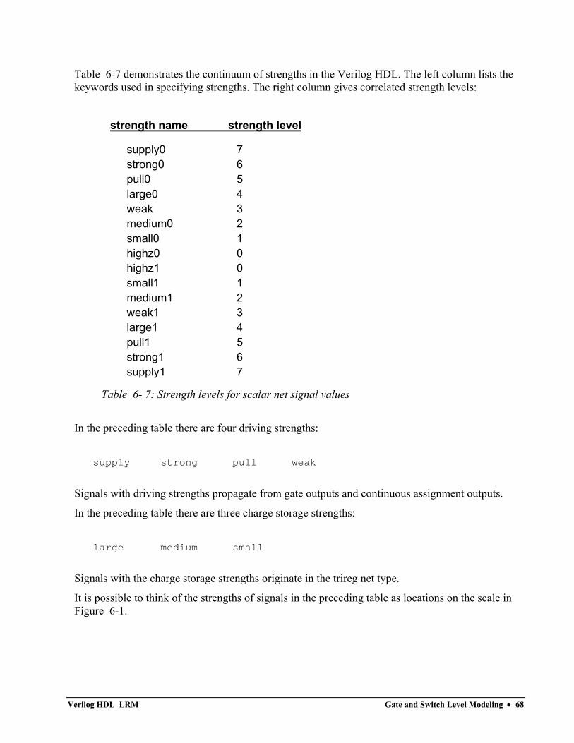
Table 6-7 demonstrates the continuum of strengths in the Verilog HDL. The left column lists the keywords used in specifying strengths. The right column gives correlated strength levels:
strength name strength level
supply0 7 strong0 6 pull0 5 large0 4 weak 3 medium0 2 small0 1 highz0 0 highz1 0 small1 1 medium1 2 weak1 3 large1 4 pull1 5 strong1 6 supply1 7
Table 6- 7: Strength levels for scalar net signal values
In the preceding table there are four driving strengths:
supply strong pull weak
Signals with driving strengths propagate from gate outputs and continuous assignment outputs.
In the preceding table there are three charge storage strengths:
large medium small
Signals with the charge storage strengths originate in the trireg net type.
It is possible to think of the strengths of signals in the preceding table as locations on the scale in Figure 6-1.
Verilog HDL LRM Gate and Switch Level Modeling • 68
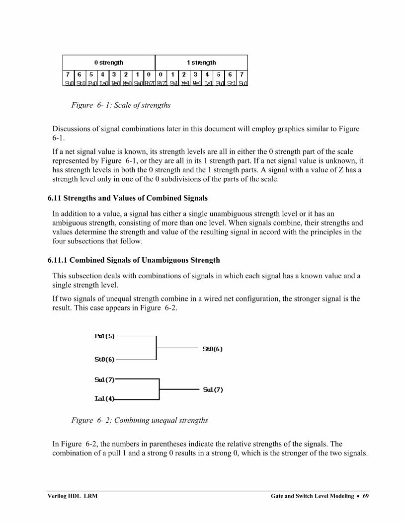
Figure 6- 1: Scale of strengths
Discussions of signal combinations later in this document will employ graphics similar to Figure 6-1.
If a net signal value is known, its strength levels are all in either the 0 strength part of the scale represented by Figure 6-1, or they are all in its 1 strength part. If a net signal value is unknown, it has strength levels in both the 0 strength and the 1 strength parts. A signal with a value of Z has a strength level only in one of the 0 subdivisions of the parts of the scale.
6.11 Strengths and Values of Combined Signals
In addition to a value, a signal has either a single unambiguous strength level or it has an ambiguous strength, consisting of more than one level. When signals combine, their strengths and values determine the strength and value of the resulting signal in accord with the principles in the four subsections that follow.
6.11.1 Combined Signals of Unambiguous Strength
This subsection deals with combinations of signals in which each signal has a known value and a single strength level.
If two signals of unequal strength combine in a wired net configuration, the stronger signal is the result. This case appears in Figure 6-2.
Figure 6- 2: Combining unequal strengths
In Figure 6-2, the numbers in parentheses indicate the relative strengths of the signals. The combination of a pull 1 and a strong 0 results in a strong 0, which is the stronger of the two signals.
Verilog HDL LRM Gate and Switch Level Modeling • 69
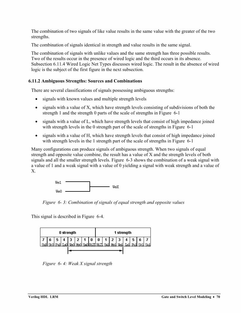
The combination of two signals of like value results in the same value with the greater of the two strengths.
The combination of signals identical in strength and value results in the same signal.
The combination of signals with unlike values and the same strength has three possible results. Two of the results occur in the presence of wired logic and the third occurs in its absence. Subsection 6.11.4 Wired Logic Net Types discusses wired logic. The result in the absence of wired logic is the subject of the first figure in the next subsection.
6.11.2 Ambiguous Strengths: Sources and Combinations
There are several classifications of signals possessing ambiguous strengths:
• signals with known values and multiple strength levels
• signals with a value of X, which have strength levels consisting of subdivisions of both the strength 1 and the strength 0 parts of the scale of strengths in Figure 6-1
• signals with a value of L, which have strength levels that consist of high impedance joined with strength levels in the 0 strength part of the scale of strengths in Figure 6-1
• signals with a value of H, which have strength levels that consist of high impedance joined with strength levels in the 1 strength part of the scale of strengths in Figure 6-1
Many configurations can produce signals of ambiguous strength. When two signals of equal strength and opposite value combine, the result has a value of X and the strength levels of both signals and all the smaller strength levels. Figure 6-3 shows the combination of a weak signal with a value of 1 and a weak signal with a value of 0 yielding a signal with weak strength and a value of X.
Figure 6- 3: Combination of signals of equal strength and opposite values
This signal is described in Figure 6-4.
Figure 6- 4: Weak X signal strength
Verilog HDL LRM Gate and Switch Level Modeling • 70
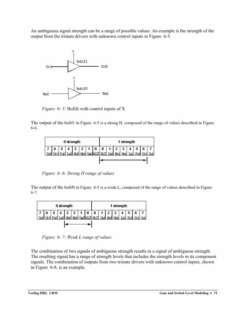
An ambiguous signal strength can be a range of possible values. An example is the strength of the output from the tristate drivers with unknown control inputs in Figure 6-5.
Figure 6- 5: Bufifs with control inputs of X
The output of the bufif1 in Figure 6-5 is a strong H, composed of the range of values described in Figure 6-6.
Figure 6- 6: Strong H range of values
The output of the bufif0 in Figure 6-5 is a weak L, composed of the range of values described in Figure 6-7.
Figure 6- 7: Weak L range of values
The combination of two signals of ambiguous strength results in a signal of ambiguous strength. The resulting signal has a range of strength levels that includes the strength levels in its component signals. The combination of outputs from two tristate drivers with unknown control inputs, shown in Figure 6-8, is an example.
Verilog HDL LRM Gate and Switch Level Modeling • 71
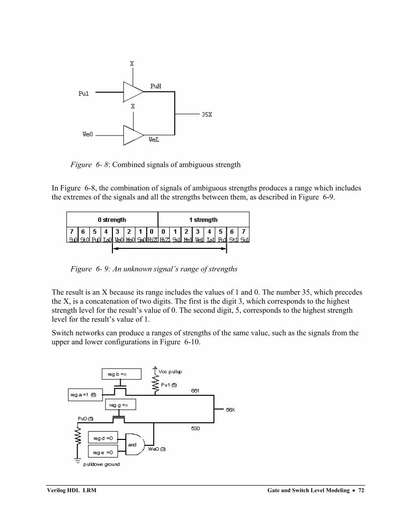
Figure 6- 8: Combined signals of ambiguous strength
In Figure 6-8, the combination of signals of ambiguous strengths produces a range which includes the extremes of the signals and all the strengths between them, as described in Figure 6-9.
Figure 6- 9: An unknown signal’s range of strengths
The result is an X because its range includes the values of 1 and 0. The number 35, which precedes the X, is a concatenation of two digits. The first is the digit 3, which corresponds to the highest strength level for the result’s value of 0. The second digit, 5, corresponds to the highest strength level for the result’s value of 1.
Switch networks can produce a ranges of strengths of the same value, such as the signals from the upper and lower configurations in Figure 6-10.
Verilog HDL LRM Gate and Switch Level Modeling • 72
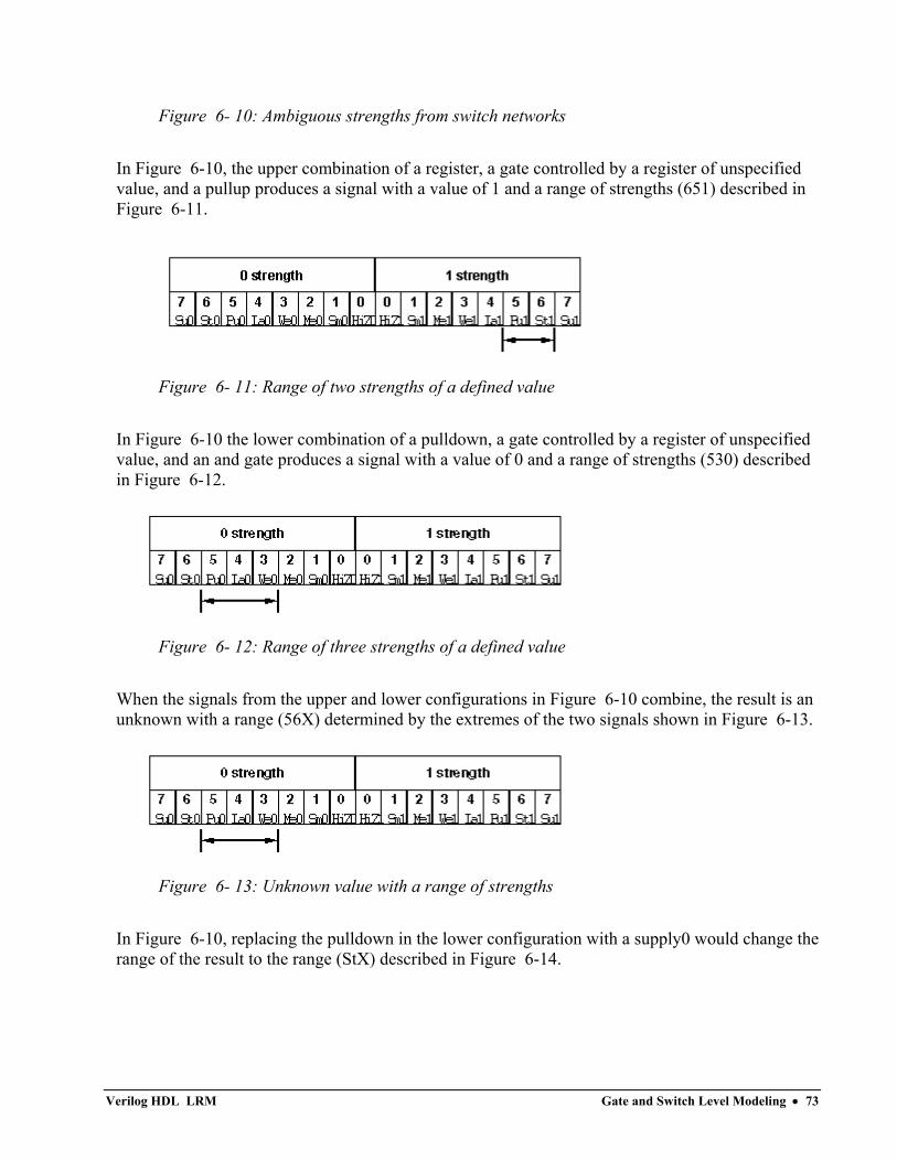
Figure 6- 10: Ambiguous strengths from switch networks
In Figure 6-10, the upper combination of a register, a gate controlled by a register of unspecified value, and a pullup produces a signal with a value of 1 and a range of strengths (651) described in Figure 6-11.
Figure 6- 11: Range of two strengths of a defined value
In Figure 6-10 the lower combination of a pulldown, a gate controlled by a register of unspecified value, and an and gate produces a signal with a value of 0 and a range of strengths (530) described in Figure 6-12.
Figure 6- 12: Range of three strengths of a defined value
When the signals from the upper and lower configurations in Figure 6-10 combine, the result is an unknown with a range (56X) determined by the extremes of the two signals shown in Figure 6-13.
Figure 6- 13: Unknown value with a range of strengths
In Figure 6-10, replacing the pulldown in the lower configuration with a supply0 would change the range of the result to the range (StX) described in Figure 6-14.
Verilog HDL LRM Gate and Switch Level Modeling • 73
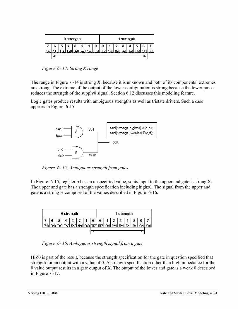
Figure 6- 14: Strong X range
The range in Figure 6-14 is strong X, because it is unknown and both of its components’ extremes are strong. The extreme of the output of the lower configuration is strong because the lower pmos reduces the strength of the supply0 signal. Section 6.12 discusses this modeling feature.
Logic gates produce results with ambiguous strengths as well as tristate drivers. Such a case appears in Figure 6-15.
Figure 6- 15: Ambiguous strength from gates
In Figure 6-15, register b has an unspecified value, so its input to the upper and gate is strong X. The upper and gate has a strength specification including highz0. The signal from the upper and gate is a strong H composed of the values described in Figure 6-16.
Figure 6- 16: Ambiguous strength signal from a gate
HiZ0 is part of the result, because the strength specification for the gate in question specified that strength for an output with a value of 0. A strength specification other than high impedance for the 0 value output results in a gate output of X. The output of the lower and gate is a weak 0 described in Figure 6-17.
Verilog HDL LRM Gate and Switch Level Modeling • 74
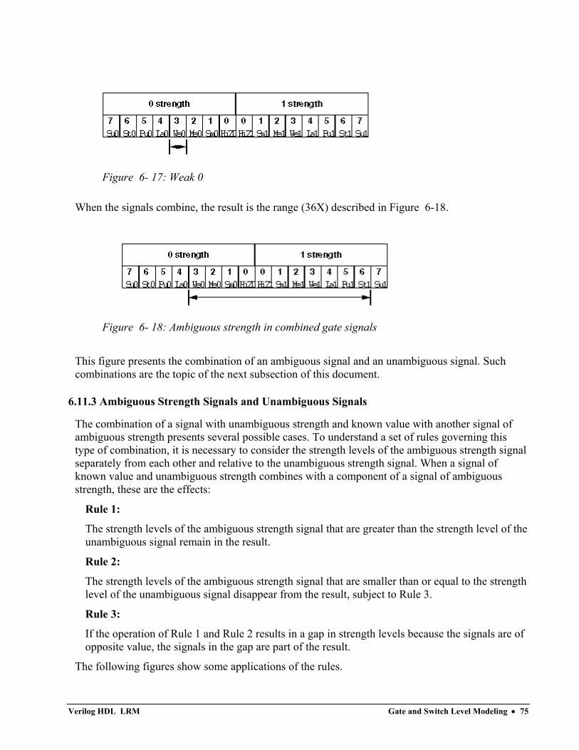
Figure 6- 17: Weak 0
When the signals combine, the result is the range (36X) described in Figure 6-18.
Figure 6- 18: Ambiguous strength in combined gate signals
This figure presents the combination of an ambiguous signal and an unambiguous signal. Such combinations are the topic of the next subsection of this document.
6.11.3 Ambiguous Strength Signals and Unambiguous Signals
The combination of a signal with unambiguous strength and known value with another signal of ambiguous strength presents several possible cases. To understand a set of rules governing this type of combination, it is necessary to consider the strength levels of the ambiguous strength signal separately from each other and relative to the unambiguous strength signal. When a signal of known value and unambiguous strength combines with a component of a signal of ambiguous strength, these are the effects:
Rule 1:
The strength levels of the ambiguous strength signal that are greater than the strength level of the unambiguous signal remain in the result.
Rule 2:
The strength levels of the ambiguous strength signal that are smaller than or equal to the strength level of the unambiguous signal disappear from the result, subject to Rule 3.
Rule 3:
If the operation of Rule 1 and Rule 2 results in a gap in strength levels because the signals are of opposite value, the signals in the gap are part of the result.
The following figures show some applications of the rules.
Verilog HDL LRM Gate and Switch Level Modeling • 75
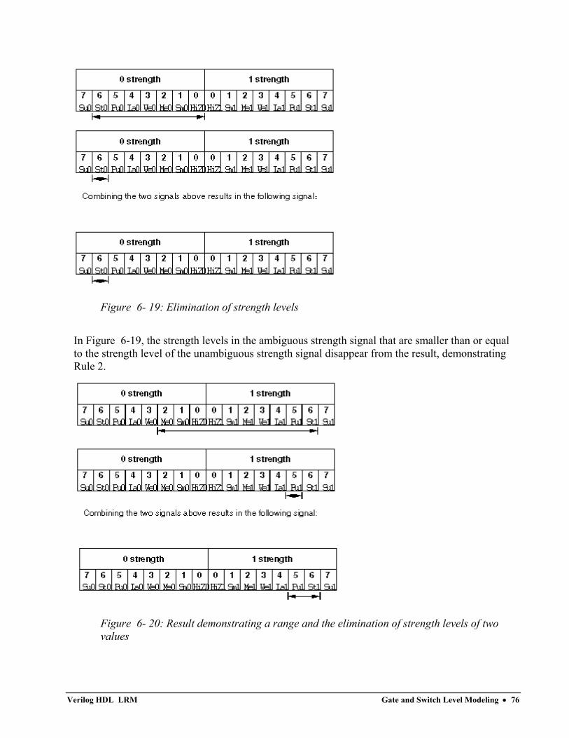
Figure 6- 19: Elimination of strength levels
In Figure 6-19, the strength levels in the ambiguous strength signal that are smaller than or equal to the strength level of the unambiguous strength signal disappear from the result, demonstrating Rule 2.
Figure 6- 20: Result demonstrating a range and the elimination of strength levels of two values
Verilog HDL LRM Gate and Switch Level Modeling • 76
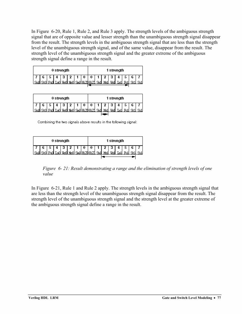
In Figure 6-20, Rule 1, Rule 2, and Rule 3 apply. The strength levels of the ambiguous strength signal that are of opposite value and lesser strength than the unambiguous strength signal disappear from the result. The strength levels in the ambiguous strength signal that are less than the strength level of the unambiguous strength signal, and of the same value, disappear from the result. The strength level of the unambiguous strength signal and the greater extreme of the ambiguous strength signal define a range in the result.
Figure 6- 21: Result demonstrating a range and the elimination of strength levels of one value
In Figure 6-21, Rule 1 and Rule 2 apply. The strength levels in the ambiguous strength signal that are less than the strength level of the unambiguous strength signal disappear from the result. The strength level of the unambiguous strength signal and the strength level at the greater extreme of the ambiguous strength signal define a range in the result.
Verilog HDL LRM Gate and Switch Level Modeling • 77
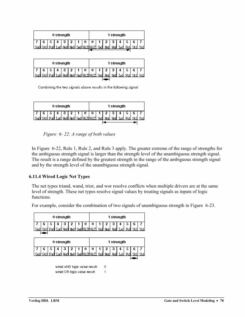
Figure 6- 22: A range of both values
In Figure 6-22, Rule 1, Rule 2, and Rule 3 apply. The greater extreme of the range of strengths for the ambiguous strength signal is larger than the strength level of the unambiguous strength signal. The result is a range defined by the greatest strength in the range of the ambiguous strength signal and by the strength level of the unambiguous strength signal.
6.11.4 Wired Logic Net Types
The net types triand, wand, trior, and wor resolve conflicts when multiple drivers are at the same level of strength. These net types resolve signal values by treating signals as inputs of logic functions.
For example, consider the combination of two signals of unambiguous strength in Figure 6-23.
Verilog HDL LRM Gate and Switch Level Modeling • 78
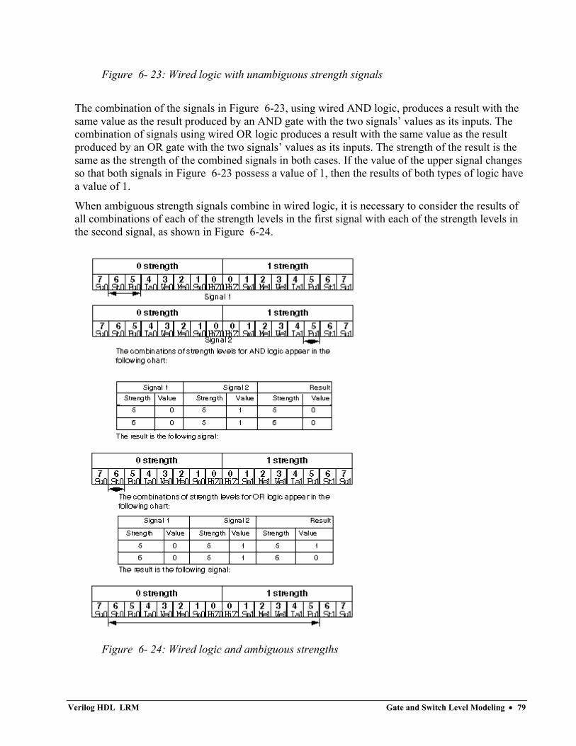
Figure 6- 23: Wired logic with unambiguous strength signals
The combination of the signals in Figure 6-23, using wired AND logic, produces a result with the same value as the result produced by an AND gate with the two signals’ values as its inputs. The combination of signals using wired OR logic produces a result with the same value as the result produced by an OR gate with the two signals’ values as its inputs. The strength of the result is the same as the strength of the combined signals in both cases. If the value of the upper signal changes so that both signals in Figure 6-23 possess a value of 1, then the results of both types of logic have a value of 1.
When ambiguous strength signals combine in wired logic, it is necessary to consider the results of all combinations of each of the strength levels in the first signal with each of the strength levels in the second signal, as shown in Figure 6-24.
Figure 6- 24: Wired logic and ambiguous strengths
Verilog HDL LRM Gate and Switch Level Modeling • 79
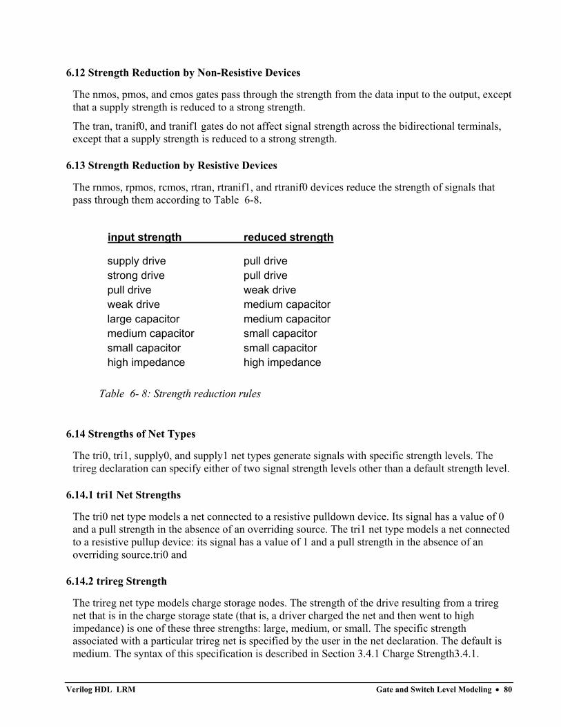
6.12 Strength Reduction by Non-Resistive Devices
The nmos, pmos, and cmos gates pass through the strength from the data input to the output, except that a supply strength is reduced to a strong strength.
The tran, tranif0, and tranif1 gates do not affect signal strength across the bidirectional terminals, except that a supply strength is reduced to a strong strength.
6.13 Strength Reduction by Resistive Devices
The rnmos, rpmos, rcmos, rtran, rtranif1, and rtranif0 devices reduce the strength of signals that pass through them according to Table 6-8.
input strength reduced strength
supply drive pull drive strong drive pull drive pull drive weak drive weak drive medium capacitor large capacitor medium capacitor medium capacitor small capacitor small capacitor small capacitor high impedance high impedance
Table 6- 8: Strength reduction rules
6.14 Strengths of Net Types
The tri0, tri1, supply0, and supply1 net types generate signals with specific strength levels. The trireg declaration can specify either of two signal strength levels other than a default strength level.
6.14.1 tri1 Net Strengths
The tri0 net type models a net connected to a resistive pulldown device. Its signal has a value of 0 and a pull strength in the absence of an overriding source. The tri1 net type models a net connected to a resistive pullup device: its signal has a value of 1 and a pull strength in the absence of an overriding source.tri0 and
6.14.2 trireg Strength
The trireg net type models charge storage nodes. The strength of the drive resulting from a trireg net that is in the charge storage state (that is, a driver charged the net and then went to high impedance) is one of these three strengths: large, medium, or small. The specific strength associated with a particular trireg net is specified by the user in the net declaration. The default is medium. The syntax of this specification is described in Section 3.4.1 Charge Strength3.4.1.
Verilog HDL LRM Gate and Switch Level Modeling • 80
6.14.3 supply0 and supply1 Net Strengths
The supply0 net type models ground connections. The supply1 net type models connections to power supplies. The supply0 and supply1 net types have supply driving strengths.
6.15 Gate and Net Delays
Gate and net delays provide a means of accurately describing delays through a circuit. The gate delays specify the signal propagation delay from any gate input to the gate output. Up to three values per output can be specified. The descriptions in this chapter of each gate type give the rules for which gates can take how many delays—see Section 6.2 and, nand, nor, or, xor, and xnor Gates through Section 6.7 cmos Gates.
Net delays refer to the time it takes from any driver on the net changing value to the time when the net value is updated and propagated further. Up to three delay values per net can be specified.
For both gates and nets, the default delay is zero when no delay specification is given. When one delay value is given, then this value is used for all propagation delays associated with the gate or net. The following is an example of a delay specification with one delay:
and #(10) (out, in1, in2);
The following is an example of a delay specification with two delays:
and #(10, 12) (out, in1, in2);
When two delays are given, the first specifies the rise delay and the second specifies the fall delay. The delay when the signal changes to high impedance or to unknown is the lesser of the two delay values.
The following is an example of a delay specification with three delays:
and #(10, 12, 11) (out, in1, in2);
For a three delay specification:
• the first delay refers to the transition to the 1 value (rise delay)
• the second delay refers to the transition to the 0 value (fall delay)
• the third delay refers to the transition to the high impedance value
When a value changes to the unknown (X) value, the delay is the smallest of the three delays.
Table 6-9 summarizes the from-to propagation delay choice for the two and three delay specifications.
Verilog HDL LRM Gate and Switch Level Modeling • 81
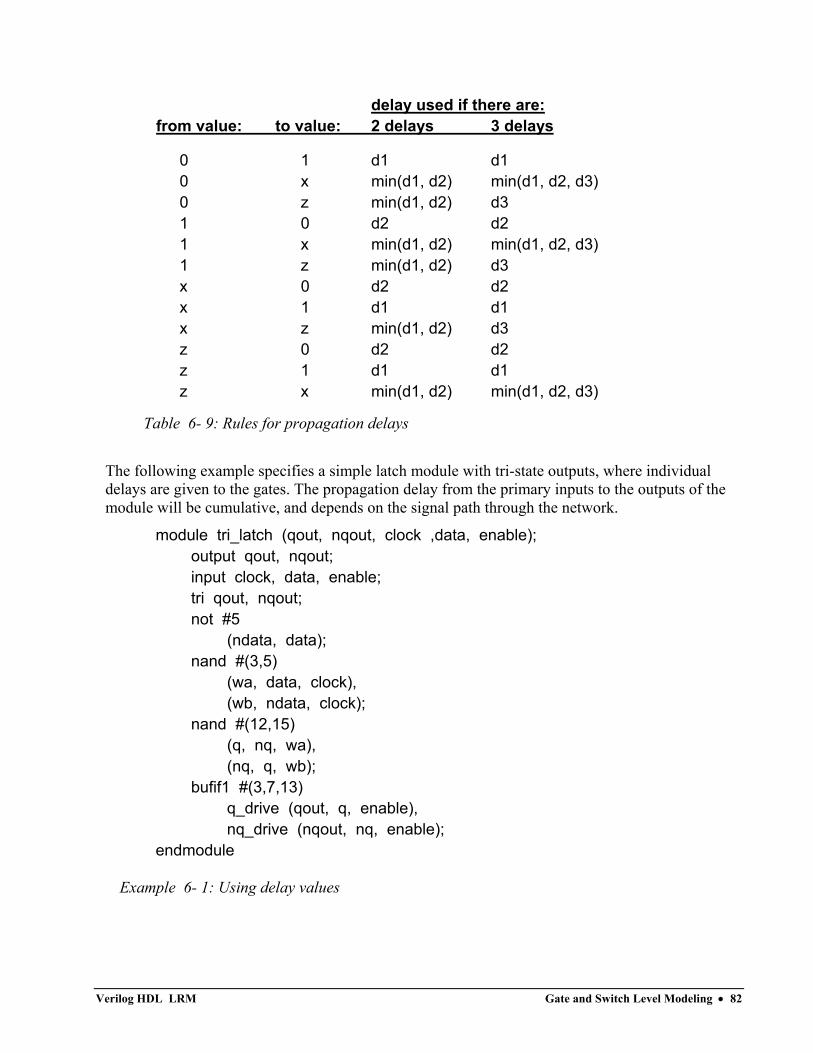
delay used if there are: from value: to value: 2 delays 3 delays
0 1 d1 d1 0 x min(d1, d2) min(d1, d2, d3) 0 z min(d1, d2) d3 1 0 d2 d2 1 x min(d1, d2) min(d1, d2, d3) 1 z min(d1, d2) d3 x 0 d2 d2 x 1 d1 d1 x z min(d1, d2) d3 z 0 d2 d2 z 1 d1 d1 z x min(d1, d2) min(d1, d2, d3)
Table 6- 9: Rules for propagation delays
The following example specifies a simple latch module with tri-state outputs, where individual delays are given to the gates. The propagation delay from the primary inputs to the outputs of the module will be cumulative, and depends on the signal path through the network.
module tri_latch (qout, nqout, clock ,data, enable); output qout, nqout; input clock, data, enable; tri qout, nqout; not #5
(ndata, data); nand #(3,5)
(wa, data, clock), (wb, ndata, clock);
nand #(12,15) (q, nq, wa), (nq, q, wb);
bufif1 #(3,7,13) q_drive (qout, q, enable), nq_drive (nqout, nq, enable);
endmodule
Example 6- 1: Using delay values
Verilog HDL LRM Gate and Switch Level Modeling • 82
6.15.1 min/typ/max Delays
The syntax for delays on gate primitives (including User-Defined Primitives), nets, and continuous assignments allows three values each for the rising, falling, and turn-off delays. The minimum, typical, and maximum values for each are specified as constant expressions separated by colons. The following example shows min/typ/max values for rising, falling, and turn-off delays:
module iobuf(io1, io2, dir); • .
• .
• .
bufif0 #(5:7:9, 8:10:12, 15:18:21) (io1, io2, dir); bufif1 #(6:8:10, 5:7:9, 13:17:19) (io2, io1, dir);
• .
• .
• .
endmodule
Example 6- 2: Syntax example for delay expressions
Tools typically default to one set of delay values (usually the typical set) for the processing of one model. A tool may or may not allow the user to select one set for a processing run.
The syntax for delay controls in procedural statements also allows minimum, typical, and maximum values. These are specified by expressions separated by colons. Example 6-3 illustrates this concept.
parameter min_hi = 97, typ_hi = 100, max_hi = 107; reg clk; always begin #(95:100:105) clk = 1; #(min_hi:typ_hi:max_hi) clk = 0; end
Example 6- 3: Delay controls in procedural statements
6.15.2 trireg Net Charge Decay
Like all nets, a trireg declaration’s delay specification can contain up to three delays. The first two delays specify the simulation time that elapses in a transition to the 1 and 0 logic states when the
Verilog HDL LRM Gate and Switch Level Modeling • 83
trireg is driven to these states by a driver. The third delay specifies the charge decay time instead of the time that elapses in a transition to the z logic state. The charge decay time specifies the simulation time that elapses between when a trireg’s drivers turn off and when its stored charge can no longer be determined.
A trireg needs no turn-off delay specification because a trireg never makes a transition to the z logic state. When a trireg’s drivers make transitions from the 1, 0, or x logic states to off, the trireg retains the previous 1, 0, or x logic state that was on its drivers. The z value does not propagate from a trireg’s drivers to a trireg. A trireg can only hold a z logic state when z is the trireg’s initial logic state or when it is forced to the z state with a force statement.
A delay specification for charge decay models a charge storage node that is not ideal, a charge storage node whose charge leaks out through its surrounding devices and connections.
This section describes the charge decay process and the delay specification for charge decay.
The charge decay process
Charge decay is the cause of transition of a 1 or 0 that is stored in a trireg to an unknown value (x) after a specified number of time units. The charge decay time is that specified number of time units.
The charge decay process begins when the trireg’s drivers turn off and the trireg starts to hold charge. The charge decay process ends under the following two conditions:
1. The specified number of time units elapse and the trireg makes a transition from 1 or 0 to x.
2. The trireg’s drivers turn on and propagate a 1, 0 or x into the trireg.
The delay specification for charge decay time
The third delay in a trireg declaration specifies the charge decay time. A three-valued delay specification in a trireg declaration has the following form:
#(d1, d2, d3)
// three delays
//(rising_delay,falling_delay,charge_decay_time)
The specification in a trireg declaration of the charge decay time must be preceded by a rise and fall delay specification. The following example shows a specification of the charge decay time in a trireg declaration:
trireg (large) #(0,0,50) cap1;
This example declares a trireg with the identifier cap1. This trireg stores a large charge. The delay specifications for the rise delay is 0, the fall delay is 0, and the charge decay time specification is 50 time units.
Verilog HDL LRM Gate and Switch Level Modeling • 84
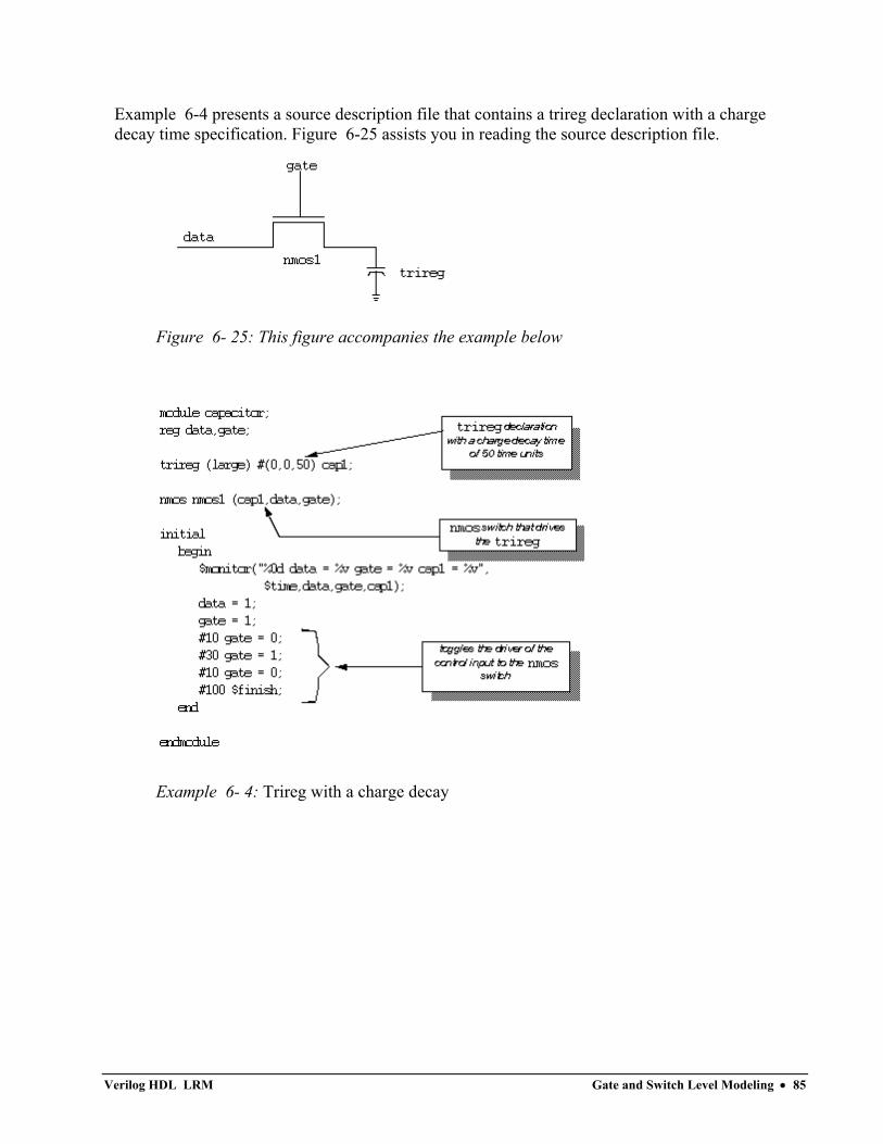
Example 6-4 presents a source description file that contains a trireg declaration with a charge decay time specification. Figure 6-25 assists you in reading the source description file.
Figure 6- 25: This figure accompanies the example below
Example 6- 4: Trireg with a charge decay
Verilog HDL LRM Gate and Switch Level Modeling • 85
User-Defined Primitives (UDPs)
7.0 UDP Overview
This chapter describes a modeling technique whereby the user can effectively augment the set of predefined gate primitives by designing and specifying new primitive elements called user-defined primitives (UDPs). Instances of these new UDPs can then be used in exactly the same manner as the gate primitives to represent the circuit being modeled.
The following two types of behavior can be represented in a user-defined primitive:
• combinational—modeled by a combinational UDP
• sequential—modeled by a sequential UDP
A sequential UDP uses the value of its inputs and the current value of its output to determine the next value of its output. Sequential UDPs provide an easy way to model sequential circuits such as flip-flops and latches. A sequential UDP can model both level-sensitive and edge-sensitive behavior.
Implementation Specific Detail: In sources compatible with some existing tools the number of inputs of each user-defined primitive may be limited by the implementation.
Each UDP has exactly one output, which can be in one of three states: 0, 1, or x. The tri-state value z is not supported. In sequential UDPs, the output always has the same value as the internal state.
Implementation Specific Detail: The maximum number of UDPs that a user can define in a model may be limited by the implementation.
7.1 Syntax
The formal syntax of the UDP definition is as follows:
<UDP> ::=primitive<name_of_UDP>(<output_terminal_name>, <input_terminal_name> <,<input_terminal_name>>*); <UDP_declaration>+ <UDP_initial_statement>? <table_definition> endprimitive
<name_of_UDP> ::=<IDENTIFIER>
<UDP_declaration>
Verilog HDL LRM User-Defined Primitives (UDPs) • 86
::=<UDP_output_declaration> ||=<reg_declaration> ||=<UDP_input_declaration>
<UDP_output_declaration> ::= output <output_terminal _name>;
<reg_declaration> reg <output_terminal_name> ;
<UDP_input_declaration> ::= input <input_terminal _name>
<,<input_terminal_name>>*);
<UDP_initial_statement> ::= initial <output_terminal_name> = <init_val> ;
<init_val> ::= 1'b0 ||= 1'b1 ||= 1'bx ||= 1 ||= 0
<table_definition> ::=table <table_entries> endtable
<table_entries> ::=<combinational_entry>+ ||=<sequential_entry>+
<combinational_entry> ::=<level_input_list>:<OUTPUT_SYMBOL>;
<sequential_entry> ::=<input_list>:<state>:<next_state>;
<input_list> ::=<level_input_list> ||=<edge_input_list>
<level_input_list> ::=<LEVEL_SYMBOL>+
Verilog HDL LRM User-Defined Primitives (UDPs) • 87
<edge_input_list> ::=<LEVEL_SYMBOL>*<edge><LEVEL_SYMBOL>*
<edge> ::=(<LEVEL_SYMBOL><LEVEL_SYMBOL>) ||=<EDGE_SYMBOL>
<state> ::=<LEVEL_SYMBOL>
<next_state> ::=<OUTPUT_SYMBOL> ||=- (This is a literal hyphen,
see Section 7.12 Summary of Symbols for more details)
Lexical tokens: <OUTPUT_SYMBOL> is one of the following: 0 1 x X <LEVEL_SYMBOL> is one of the following: 0 1 x X ? b B <EDGE_SYMBOL> is one of the following: r R f F p P n N *
Syntax 7- 1: Syntax for user-defined primitivess
7.2 UDP Definition
UDP definitions are independent of modules; they are at the same level as module definitions in the syntax hierarchy. They can appear anywhere in the source text, either before or after they are used inside a module. They MAY NOT appear between the keywords module and endmodule.
A UDP definition begins with the keyword primitive. This is followed by an identifier, which is the name of the UDP. This in turn is followed by a comma separated list of terminals enclosed in parentheses, which is followed by a semicolon.
The UDP definition header described previously is followed by terminal declarations and a state table. The UDP definition is terminated by the keyword endprimitive.
7.2.1 UDP Terminals
UDPs have multiple input terminals and exactly one output terminal; they cannot have bidirectional inout terminals.
The output terminal MUST be the first terminal in the terminal list.
All UDP terminals are scalar. No vector terminals are allowed.
Verilog HDL LRM User-Defined Primitives (UDPs) • 88
The output terminal of a sequential UDP requires an additional declaration as type reg. It is illegal to declare a reg for the output terminal of a combinational UDP.
7.2.2 UDP Declarations
UDPs must contain input and output terminal declarations. The output terminal declaration begins with the keyword output, followed by one output terminal name. The input terminal declaration begins with the keyword input, followed by one or more input terminal names.
Sequential UDPs must contain a reg declaration for the output terminal. Combinational UDPs cannot contain a reg declaration. The initial value of the output terminal reg can be specified in an initial statement in a sequential UDP.
7.2.3 Sequential UDP initial Statement
The sequential UDP initial statement specifies the value of the output terminal when simulation begins. This statement begins with the keyword initial. The statement that follows must be an assignment statement that assigns a single bit literal value to the output terminal reg.
7.2.4 UDP State Table
The state table which defines the behavior of a UDP begins with the keyword table and is terminated with the keyword endtable.
Each row of the table is created using a variety of characters which indicate input and output states. Three states—0, 1, and x—are supported. The z state is explicitly excluded from consideration in user-defined primitives. A number of special characters are defined to represent certain combinations of state possibilities. These are detailed in this chapter, in Section 7.8 Symbols to Enhance Readability.
The order of the input state fields of each row of the state table is taken directly from the terminal list in the UDP definition header. It is NOT related to the order of the input declarations.
Combinational UDPs have one field per input and one field for the output. The input fields are separated from the output field by a colon.
Sequential UDPs have an additional field inserted between the input fields and the output field. This additional field represents the current state of the UDP and is considered equivalent to the current output value. It is delimited by colons.
Each row defines the output for a particular combination of input states. If all inputs are specified as x, then the output must be specified as x. All combinations that are not explicitly specified result in a default output state of x. Each row of the table is terminated by a semicolon.
Consider the following entry from a UDP state table:
0 1 : ? : 1 ;
Verilog HDL LRM User-Defined Primitives (UDPs) • 89
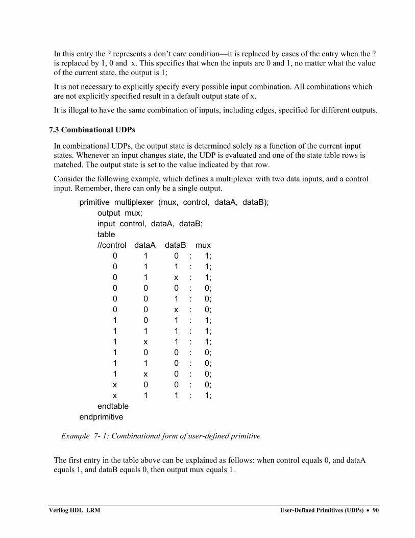
In this entry the ? represents a don’t care condition—it is replaced by cases of the entry when the ? is replaced by 1, 0 and x. This specifies that when the inputs are 0 and 1, no matter what the value of the current state, the output is 1;
It is not necessary to explicitly specify every possible input combination. All combinations which are not explicitly specified result in a default output state of x.
It is illegal to have the same combination of inputs, including edges, specified for different outputs.
7.3 Combinational UDPs
In combinational UDPs, the output state is determined solely as a function of the current input states. Whenever an input changes state, the UDP is evaluated and one of the state table rows is matched. The output state is set to the value indicated by that row.
Consider the following example, which defines a multiplexer with two data inputs, and a control input. Remember, there can only be a single output.
primitive multiplexer (mux, control, dataA, dataB); output mux; input control, dataA, dataB; table //control dataA dataB mux
0 1 0 : 1; 0 1 1 : 1; 0 1 x : 1; 0 0 0 : 0; 0 0 1 : 0; 0 0 x : 0; 1 0 1 : 1; 1 1 1 : 1; 1 x 1 : 1; 1 0 0 : 0; 1 1 0 : 0; 1 x 0 : 0; x 0 0 : 0; x 1 1 : 1;
endtable endprimitive
Example 7- 1: Combinational form of user-defined primitive
The first entry in the table above can be explained as follows: when control equals 0, and dataA equals 1, and dataB equals 0, then output mux equals 1.
Verilog HDL LRM User-Defined Primitives (UDPs) • 90
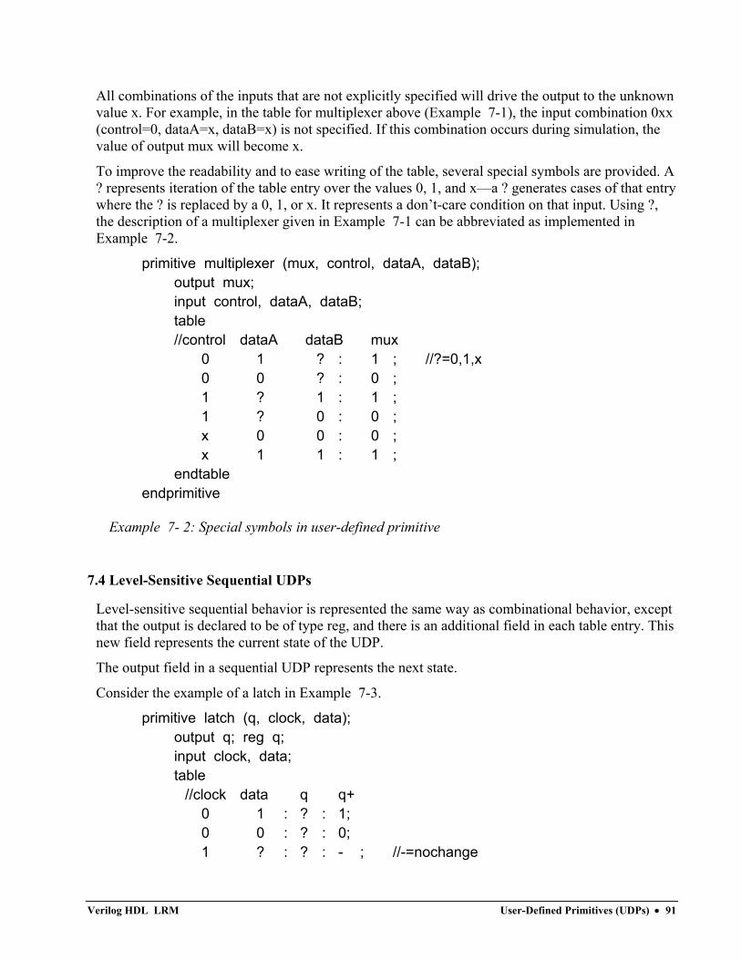
All combinations of the inputs that are not explicitly specified will drive the output to the unknown value x. For example, in the table for multiplexer above (Example 7-1), the input combination 0xx (control=0, dataA=x, dataB=x) is not specified. If this combination occurs during simulation, the value of output mux will become x.
To improve the readability and to ease writing of the table, several special symbols are provided. A ? represents iteration of the table entry over the values 0, 1, and x—a ? generates cases of that entry where the ? is replaced by a 0, 1, or x. It represents a don’t-care condition on that input. Using ?, the description of a multiplexer given in Example 7-1 can be abbreviated as implemented in Example 7-2.
primitive multiplexer (mux, control, dataA, dataB); output mux; input control, dataA, dataB; table //control dataA dataB mux
0 1 ? : 1 ; //?=0,1,x 0 0 ? : 0 ; 1 ? 1 : 1 ; 1 ? 0 : 0 ; x 0 0 : 0 ; x 1 1 : 1 ;
endtable endprimitive
Example 7- 2: Special symbols in user-defined primitive
7.4 Level-Sensitive Sequential UDPs
Level-sensitive sequential behavior is represented the same way as combinational behavior, except that the output is declared to be of type reg, and there is an additional field in each table entry. This new field represents the current state of the UDP.
The output field in a sequential UDP represents the next state.
Consider the example of a latch in Example 7-3.
primitive latch (q, clock, data); output q; reg q; input clock, data; table
//clock data q q+ 0 1 : ? : 1; 0 0 : ? : 0; 1 ? : ? : - ; //-=nochange
Verilog HDL LRM User-Defined Primitives (UDPs) • 91
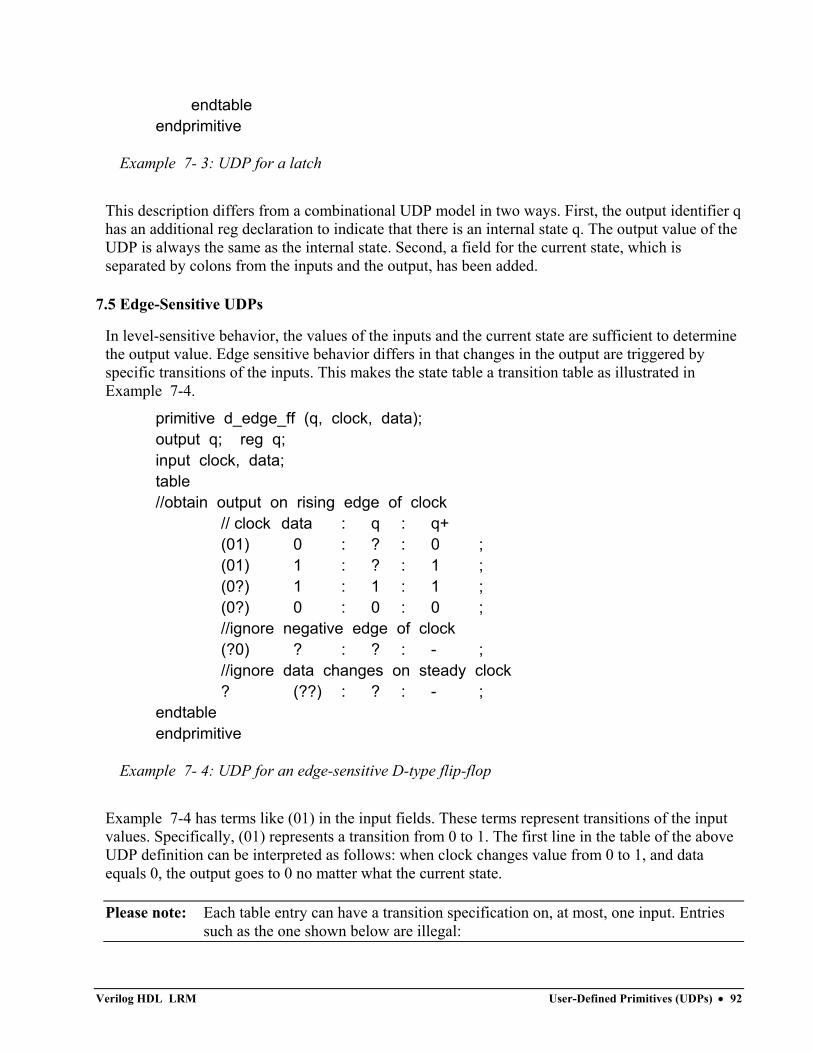
endtable endprimitive
Example 7- 3: UDP for a latch
This description differs from a combinational UDP model in two ways. First, the output identifier q has an additional reg declaration to indicate that there is an internal state q. The output value of the UDP is always the same as the internal state. Second, a field for the current state, which is separated by colons from the inputs and the output, has been added.
7.5 Edge-Sensitive UDPs
In level-sensitive behavior, the values of the inputs and the current state are sufficient to determine the output value. Edge sensitive behavior differs in that changes in the output are triggered by specific transitions of the inputs. This makes the state table a transition table as illustrated in Example 7-4.
primitive d_edge_ff (q, clock, data); output q; reg q; input clock, data; table //obtain output on rising edge of clock
// clock data : q : q+ (01) 0 : ? : 0 ; (01) 1 : ? : 1 ; (0?) 1 : 1 : 1 ; (0?) 0 : 0 : 0 ; //ignore negative edge of clock (?0) ? : ? : - ; //ignore data changes on steady clock ? (??) : ? : - ;
endtable endprimitive
Example 7- 4: UDP for an edge-sensitive D-type flip-flop
Example 7-4 has terms like (01) in the input fields. These terms represent transitions of the input values. Specifically, (01) represents a transition from 0 to 1. The first line in the table of the above UDP definition can be interpreted as follows: when clock changes value from 0 to 1, and data equals 0, the output goes to 0 no matter what the current state.
Please note: Each table entry can have a transition specification on, at most, one input. Entries such as the one shown below are illegal:
Verilog HDL LRM User-Defined Primitives (UDPs) • 92
(01)(01)0 : 0 : 1
As in the combinational and the level-sensitive entries, a ? implies iteration of the entry over the values 0, 1, and x. A dash (-) in the output column indicates no value change.
All unspecified transitions default to the output value x. Thus, in the previous example, transition of clock from 0 to x with data equal to 0 and current state equal to 1 will result in the output q going to x.
All transitions that should not affect the output MUST be explicitly specified. Otherwise, they will cause the value of the output to change to x. If the UDP is sensitive to edges of any input, the desired output state must be specified for all edges of all inputs.
7.6 Sequential UDP Initialization
The value on the output terminal of a sequential UDP can be specified with an initial statement that contains a procedural assignment statement. The initial statement is optional.
Like initial statements in modules, the initial statement in UDPs begin with the keyword initial. The valid contents of initial statements in UDPs and the valid left and right hand sides of their procedural assignment statements differ from initial statements in modules. The difference between these two types of initial statements is described in Table 7-1.
Table 7- 1: Initial statements in UDPs and modules
Example 7-5 shows a sequential UDP that contains an initial statement that specifies that output terminal q has a value of 1 at the start of the simulation
primitive srff (q,s,r); output q; input s,r; reg q; initial q = 1'b1; table
Verilog HDL LRM User-Defined Primitives (UDPs) • 93
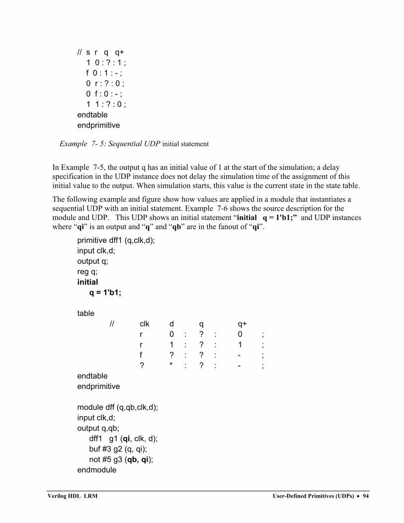
// s r q q+ 1 0 : ? : 1 ; f 0 : 1 : - ; 0 r : ? : 0 ; 0 f : 0 : - ; 1 1 : ? : 0 ; endtable endprimitive
Example 7- 5: Sequential UDP initial statement
In Example 7-5, the output q has an initial value of 1 at the start of the simulation; a delay specification in the UDP instance does not delay the simulation time of the assignment of this initial value to the output. When simulation starts, this value is the current state in the state table.
The following example and figure show how values are applied in a module that instantiates a sequential UDP with an initial statement. Example 7-6 shows the source description for the module and UDP. This UDP shows an initial statement “initial q = 1'b1;” and UDP instances where “qi” is an output and “q” and “qb” are in the fanout of “qi”.
primitive dff1 (q,clk,d); input clk,d; output q; reg q; initial q = 1'b1; table
// clk d q q+ r 0 : ? : 0 ; r 1 : ? : 1 ; f ? : ? : - ; ? * : ? : - ;
endtable endprimitive module dff (q,qb,clk,d); input clk,d; output q,qb; dff1 g1 (qi, clk, d); buf #3 g2 (q, qi); not #5 g3 (qb, qi); endmodule
Verilog HDL LRM User-Defined Primitives (UDPs) • 94
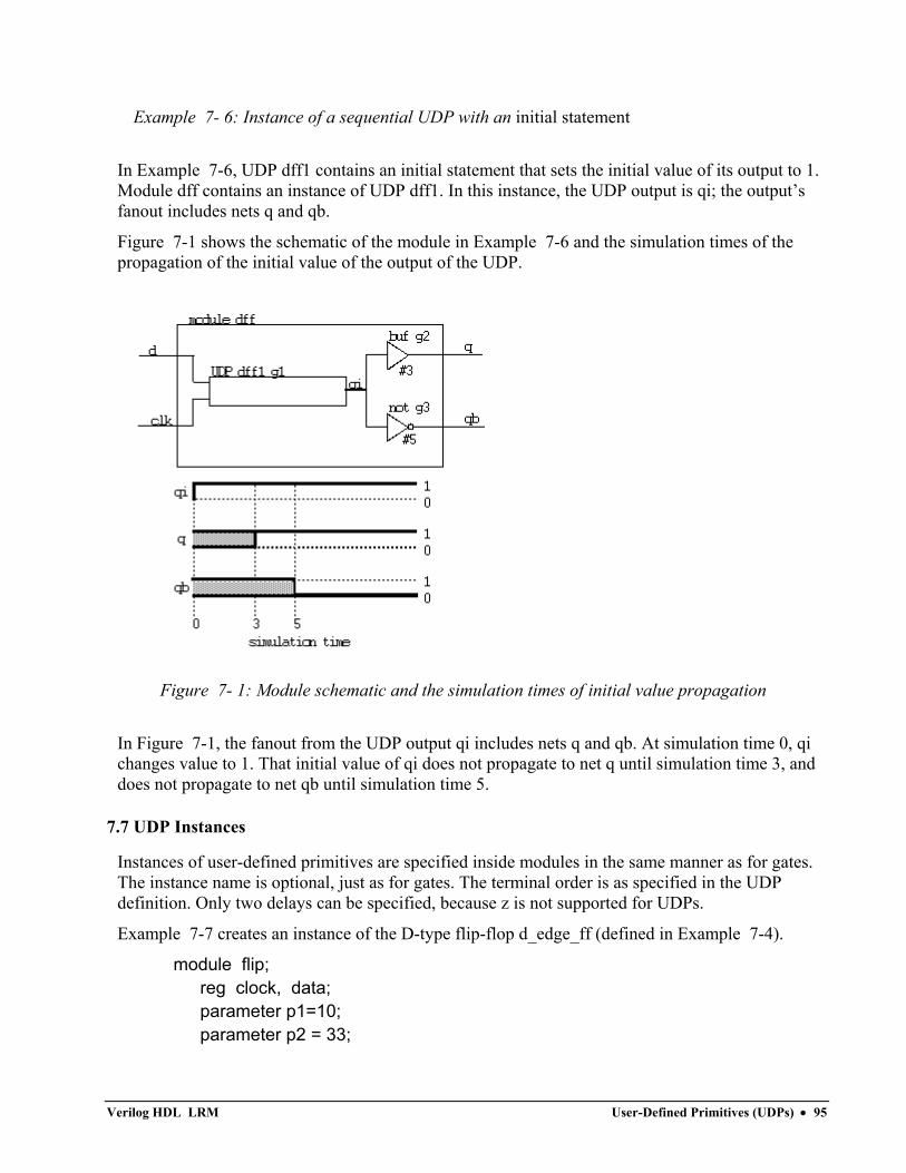
Example 7- 6: Instance of a sequential UDP with an initial statement
In Example 7-6, UDP dff1 contains an initial statement that sets the initial value of its output to 1. Module dff contains an instance of UDP dff1. In this instance, the UDP output is qi; the output’s fanout includes nets q and qb.
Figure 7-1 shows the schematic of the module in Example 7-6 and the simulation times of the propagation of the initial value of the output of the UDP.
Figure 7- 1: Module schematic and the simulation times of initial value propagation
In Figure 7-1, the fanout from the UDP output qi includes nets q and qb. At simulation time 0, qi changes value to 1. That initial value of qi does not propagate to net q until simulation time 3, and does not propagate to net qb until simulation time 5.
7.7 UDP Instances
Instances of user-defined primitives are specified inside modules in the same manner as for gates. The instance name is optional, just as for gates. The terminal order is as specified in the UDP definition. Only two delays can be specified, because z is not supported for UDPs.
Example 7-7 creates an instance of the D-type flip-flop d_edge_ff (defined in Example 7-4).
module flip; reg clock, data; parameter p1=10; parameter p2 = 33;
Verilog HDL LRM User-Defined Primitives (UDPs) • 95
parameter p3 = 12; d_edge_ff #p3 d_inst(q, clock, data); initial begin data = 1; clock = 1; end always #p1 clock = ~clock; always #p2 data = ~data; endmodule
Example 7- 7: UPD for a D-type flip-flop
7.8 Symbols to Enhance Readability
Like ?, there are several symbols that can be used in UDP definitions to make the description more readable. The symbols described in Table 7-2 are used in Example 7-8.
Symbol Interpretation Explanation
b 0 or 1 like ?, except x is excluded
r (01) rising edge on an input
f (10) falling edge on an input
p (01) or rising edges, including (0x) or (x1) or unknown (1z) or (z1)
n (10) or falling edges, including (1x) or (x0) or unknown (0z) or (z0)
* (??) all transitions
Table 7- 2: Symbols for readability
Verilog HDL LRM User-Defined Primitives (UDPs) • 96
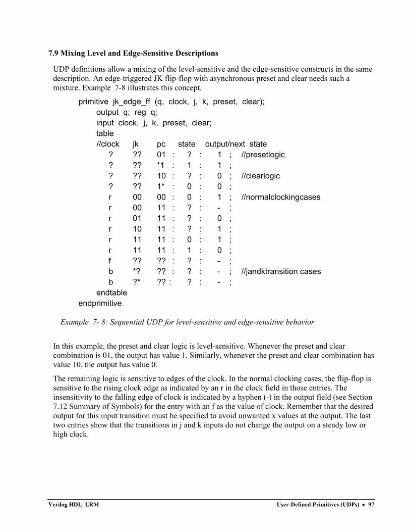
7.9 Mixing Level and Edge-Sensitive Descriptions
UDP definitions allow a mixing of the level-sensitive and the edge-sensitive constructs in the same description. An edge-triggered JK flip-flop with asynchronous preset and clear needs such a mixture. Example 7-8 illustrates this concept.
primitive jk_edge_ff (q, clock, j, k, preset, clear); output q; reg q; input clock, j, k, preset, clear; table //clock jk pc state output/next state
? ?? 01 : ? : 1 ; //presetlogic ? ?? *1 : 1 : 1 ; ? ?? 10 : ? : 0 ; //clearlogic ? ?? 1* : 0 : 0 ; r 00 00 : 0 : 1 ; //normalclockingcases r 00 11 : ? : - ; r 01 11 : ? : 0 ; r 10 11 : ? : 1 ; r 11 11 : 0 : 1 ; r 11 11 : 1 : 0 ; f ?? ?? : ? : - ; b *? ?? : ? : - ; //jandktransition cases b ?* ?? : ? : - ;
endtable endprimitive
Example 7- 8: Sequential UDP for level-sensitive and edge-sensitive behavior
In this example, the preset and clear logic is level-sensitive. Whenever the preset and clear combination is 01, the output has value 1. Similarly, whenever the preset and clear combination has value 10, the output has value 0.
The remaining logic is sensitive to edges of the clock. In the normal clocking cases, the flip-flop is sensitive to the rising clock edge as indicated by an r in the clock field in those entries. The insensitivity to the falling edge of clock is indicated by a hyphen (-) in the output field (see Section 7.12 Summary of Symbols) for the entry with an f as the value of clock. Remember that the desired output for this input transition must be specified to avoid unwanted x values at the output. The last two entries show that the transitions in j and k inputs do not change the output on a steady low or high clock.
Verilog HDL LRM User-Defined Primitives (UDPs) • 97
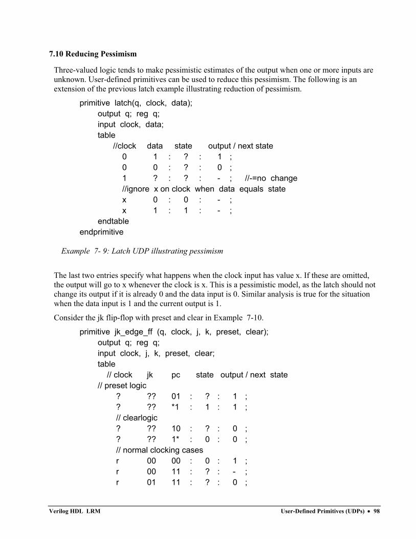
7.10 Reducing Pessimism
Three-valued logic tends to make pessimistic estimates of the output when one or more inputs are unknown. User-defined primitives can be used to reduce this pessimism. The following is an extension of the previous latch example illustrating reduction of pessimism.
primitive latch(q, clock, data); output q; reg q; input clock, data; table
//clock data state output / next state 0 1 : ? : 1 ; 0 0 : ? : 0 ; 1 ? : ? : - ; //-=no change //ignore x on clock when data equals state x 0 : 0 : - ; x 1 : 1 : - ;
endtable endprimitive
Example 7- 9: Latch UDP illustrating pessimism
The last two entries specify what happens when the clock input has value x. If these are omitted, the output will go to x whenever the clock is x. This is a pessimistic model, as the latch should not change its output if it is already 0 and the data input is 0. Similar analysis is true for the situation when the data input is 1 and the current output is 1.
Consider the jk flip-flop with preset and clear in Example 7-10.
primitive jk_edge_ff (q, clock, j, k, preset, clear); output q; reg q; input clock, j, k, preset, clear; table // clock jk pc state output / next state // preset logic
? ?? 01 : ? : 1 ; ? ?? *1 : 1 : 1 ; // clearlogic ? ?? 10 : ? : 0 ; ? ?? 1* : 0 : 0 ; // normal clocking cases r 00 00 : 0 : 1 ; r 00 11 : ? : - ; r 01 11 : ? : 0 ;
Verilog HDL LRM User-Defined Primitives (UDPs) • 98
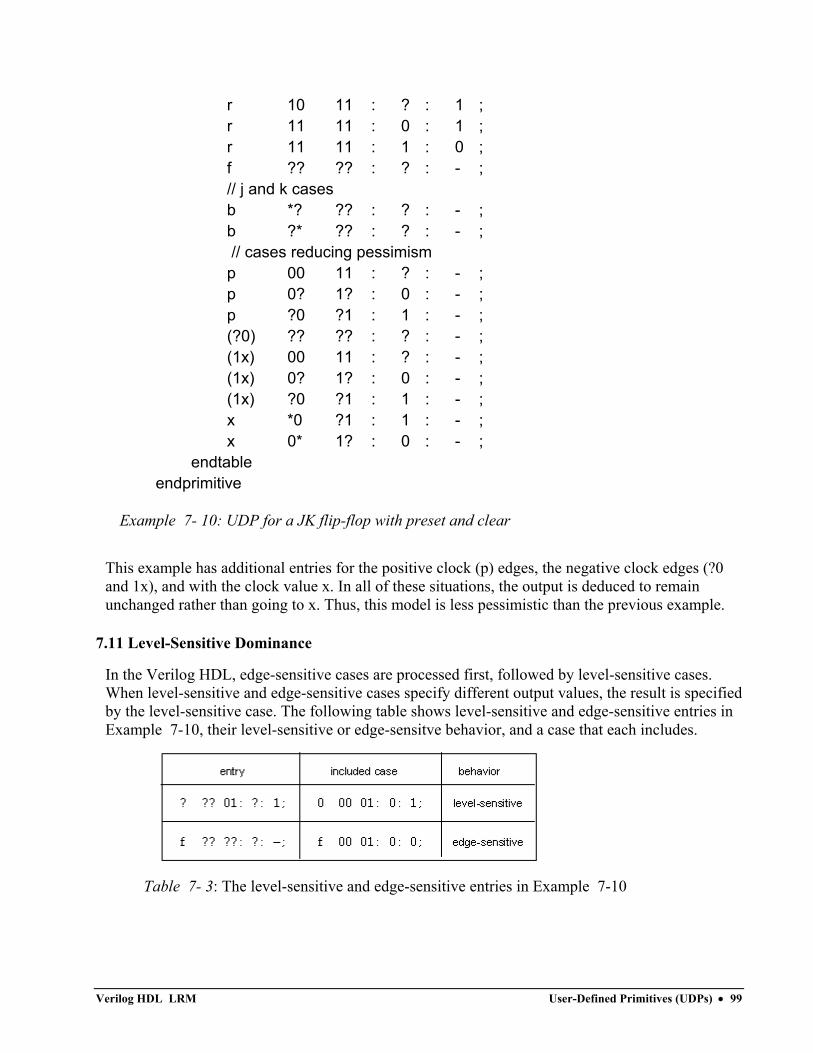
r 10 11 : ? : 1 ; r 11 11 : 0 : 1 ; r 11 11 : 1 : 0 ; f ?? ?? : ? : - ; // j and k cases b *? ?? : ? : - ; b ?* ?? : ? : - ; // cases reducing pessimism p 00 11 : ? : - ; p 0? 1? : 0 : - ; p ?0 ?1 : 1 : - ; (?0) ?? ?? : ? : - ; (1x) 00 11 : ? : - ; (1x) 0? 1? : 0 : - ; (1x) ?0 ?1 : 1 : - ; x *0 ?1 : 1 : - ; x 0* 1? : 0 : - ;
endtable endprimitive
Example 7- 10: UDP for a JK flip-flop with preset and clear
This example has additional entries for the positive clock (p) edges, the negative clock edges (?0 and 1x), and with the clock value x. In all of these situations, the output is deduced to remain unchanged rather than going to x. Thus, this model is less pessimistic than the previous example.
7.11 Level-Sensitive Dominance
In the Verilog HDL, edge-sensitive cases are processed first, followed by level-sensitive cases. When level-sensitive and edge-sensitive cases specify different output values, the result is specified by the level-sensitive case. The following table shows level-sensitive and edge-sensitive entries in Example 7-10, their level-sensitive or edge-sensitve behavior, and a case that each includes.
Table 7- 3: The level-sensitive and edge-sensitive entries in Example 7-10
Verilog HDL LRM User-Defined Primitives (UDPs) • 99
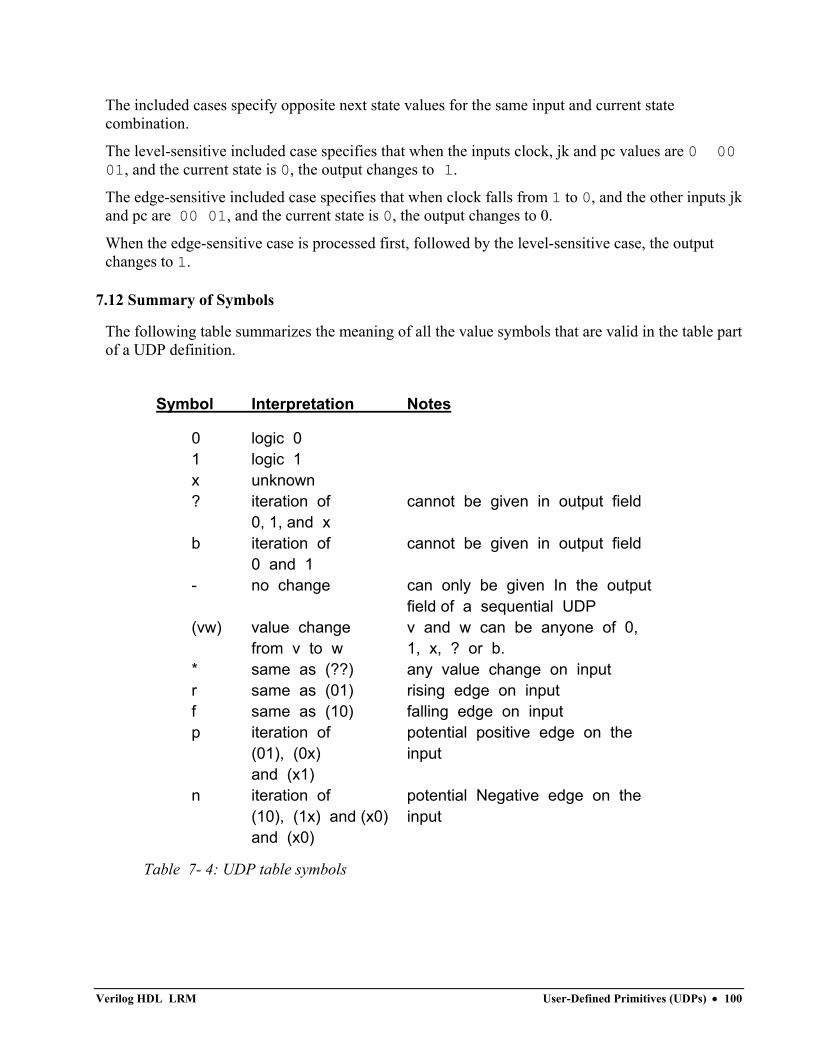
The included cases specify opposite next state values for the same input and current state combination.
The level-sensitive included case specifies that when the inputs clock, jk and pc values are 0 00 01, and the current state is 0, the output changes to 1.
The edge-sensitive included case specifies that when clock falls from 1 to 0, and the other inputs jk and pc are 00 01, and the current state is 0, the output changes to 0.
When the edge-sensitive case is processed first, followed by the level-sensitive case, the output changes to 1.
7.12 Summary of Symbols
The following table summarizes the meaning of all the value symbols that are valid in the table part of a UDP definition.
Symbol Interpretation Notes
0 logic 0 1 logic 1 x unknown ? iteration of cannot be given in output field 0, 1, and x b iteration of cannot be given in output field 0 and 1 - no change can only be given In the output field of a sequential UDP (vw) value change v and w can be anyone of 0, from v to w 1, x, ? or b. * same as (??) any value change on input r same as (01) rising edge on input f same as (10) falling edge on input p iteration of potential positive edge on the (01), (0x) input and (x1) n iteration of potential Negative edge on the (10), (1x) and (x0) input and (x0)
Table 7- 4: UDP table symbols
Verilog HDL LRM User-Defined Primitives (UDPs) • 100
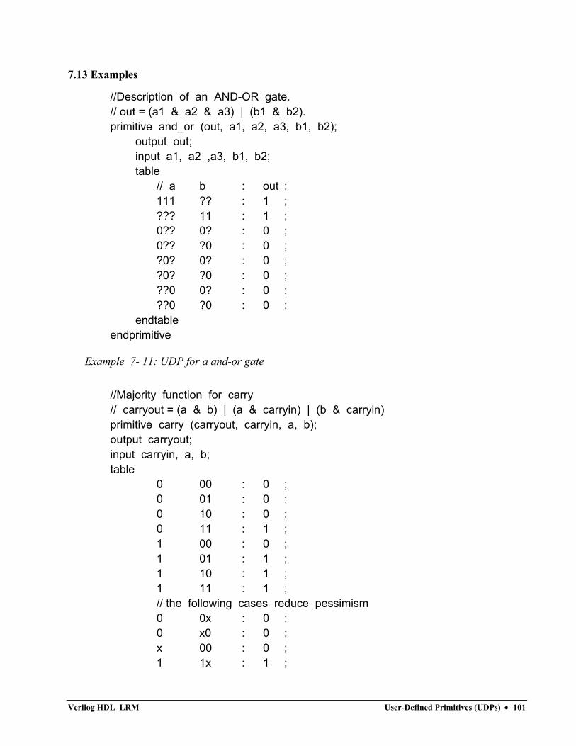
7.13 Examples
//Description of an AND-OR gate. // out = (a1 & a2 & a3) | (b1 & b2). primitive and_or (out, a1, a2, a3, b1, b2);
output out; input a1, a2 ,a3, b1, b2; table
// a b : out ; 111 ?? : 1 ; ??? 11 : 1 ; 0?? 0? : 0 ; 0?? ?0 : 0 ; ?0? 0? : 0 ; ?0? ?0 : 0 ; ??0 0? : 0 ; ??0 ?0 : 0 ;
endtable endprimitive
Example 7- 11: UDP for a and-or gate
//Majority function for carry // carryout = (a & b) | (a & carryin) | (b & carryin) primitive carry (carryout, carryin, a, b); output carryout; input carryin, a, b; table
0 00 : 0 ; 0 01 : 0 ; 0 10 : 0 ; 0 11 : 1 ; 1 00 : 0 ; 1 01 : 1 ; 1 10 : 1 ; 1 11 : 1 ; // the following cases reduce pessimism 0 0x : 0 ; 0 x0 : 0 ; x 00 : 0 ; 1 1x : 1 ;
Verilog HDL LRM User-Defined Primitives (UDPs) • 101
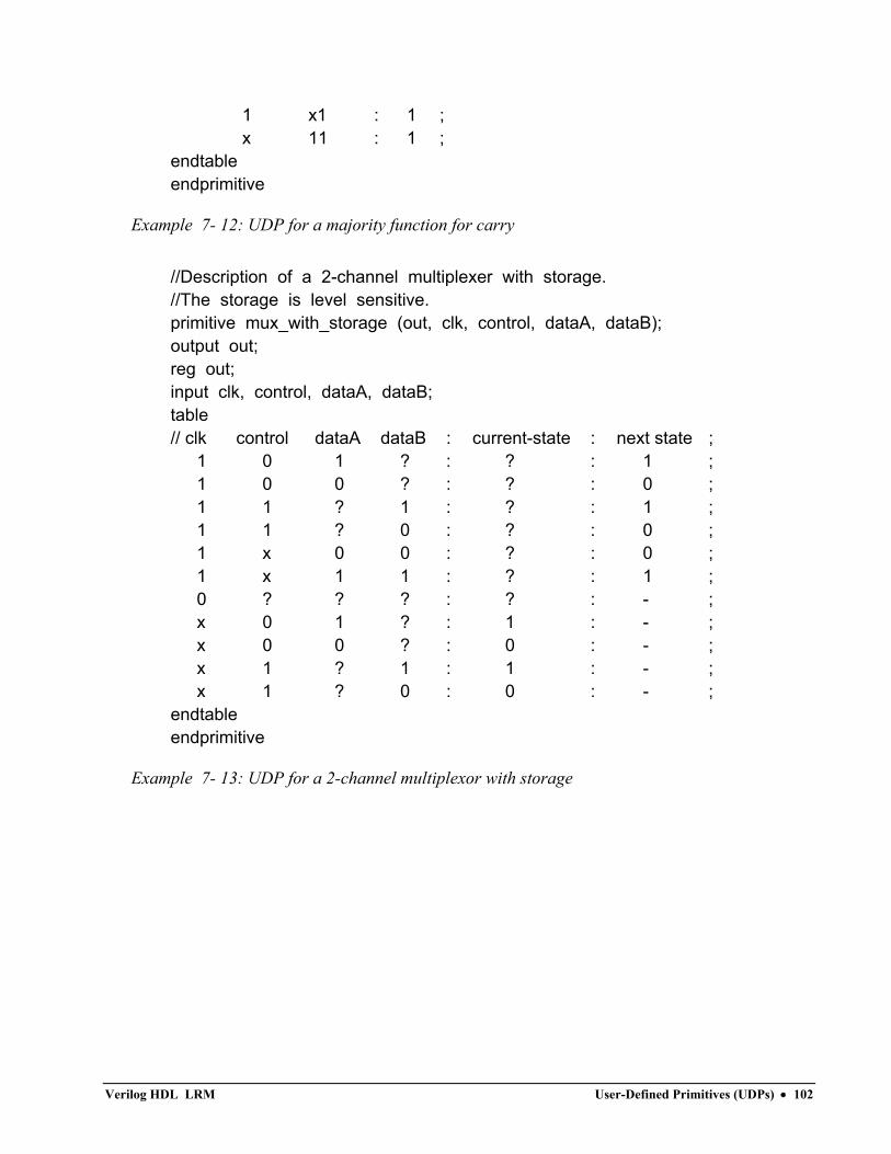
1 x1 : 1 ; x 11 : 1 ;
endtable endprimitive
Example 7- 12: UDP for a majority function for carry
//Description of a 2-channel multiplexer with storage. //The storage is level sensitive. primitive mux_with_storage (out, clk, control, dataA, dataB); output out; reg out; input clk, control, dataA, dataB; table // clk control dataA dataB : current-state : next state ;
1 0 1 ? : ? : 1 ; 1 0 0 ? : ? : 0 ; 1 1 ? 1 : ? : 1 ; 1 1 ? 0 : ? : 0 ; 1 x 0 0 : ? : 0 ; 1 x 1 1 : ? : 1 ; 0 ? ? ? : ? : - ; x 0 1 ? : 1 : - ; x 0 0 ? : 0 : - ; x 1 ? 1 : 1 : - ; x 1 ? 0 : 0 : - ;
endtable endprimitive
Example 7- 13: UDP for a 2-channel multiplexor with storage
Verilog HDL LRM User-Defined Primitives (UDPs) • 102
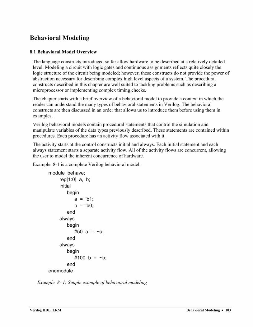
Behavioral Modeling
8.1 Behavioral Model Overview
The language constructs introduced so far allow hardware to be described at a relatively detailed level. Modeling a circuit with logic gates and continuous assignments reflects quite closely the logic structure of the circuit being modeled; however, these constructs do not provide the power of abstraction necessary for describing complex high level aspects of a system. The procedural constructs described in this chapter are well suited to tackling problems such as describing a microprocessor or implementing complex timing checks.
The chapter starts with a brief overview of a behavioral model to provide a context in which the reader can understand the many types of behavioral statements in Verilog. The behavioral constructs are then discussed in an order that allows us to introduce them before using them in examples.
Verilog behavioral models contain procedural statements that control the simulation and manipulate variables of the data types previously described. These statements are contained within procedures. Each procedure has an activity flow associated with it.
The activity starts at the control constructs initial and always. Each initial statement and each always statement starts a separate activity flow. All of the activity flows are concurrent, allowing the user to model the inherent concurrence of hardware.
Example 8-1 is a complete Verilog behavioral model.
module behave; reg[1:0] a, b; initial
begin a = 'b1; b = 'b0;
end always
begin #50 a = ~a;
end always
begin #100 b = ~b;
end endmodule
Example 8- 1: Simple example of behavioral modeling
Verilog HDL LRM Behavioral Modeling • 103
During simulation of this model, all of the flows defined by the initial and always statements start together at simulation time zero. The initial statements execute once, and the always statements execute repetitively.
In this model, the register variables a and b initialize to binary 1 and 0 respectively at simulation time zero. The initial statement is then complete and does not execute again during this simulation run. This initial statement contains a begin-end block (also called a sequential block) of statements. In this begin-end block a is initialized first, followed by b.
The always statements also start at time zero, but the values of the variables do not change until the times specified by the delay controls (introduced by #) have gone by. Thus, register a inverts after 50 time units, and register b inverts after 100 time units. Since the always statements repeat, this model produces two square waves. Register a toggles with a period of 100 time units, and register b toggles with a period of 200 time units. The two always statements proceed concurrently throughout the entire simulation run.
8.2 Procedural Assignments
As described in Chapter 5, 5.2 Procedural Assignments, procedural assignments are for updating reg, integer, time, and memory variables.
There is a significant difference between procedural assignments and continuous assignments:
• Continuous assignments drive net variables and are evaluated and updated whenever an input operand changes value.
• Procedural assignments update the value of register variables under the control of the procedural flow constructs that surround them.
The right-hand side of a procedural assignment can be any expression that evaluates to a value. However, part-selects on the right-hand side must have constant indices. The left-hand side indicates the variable that receives the assignment from the right-hand side. The left-hand side of a procedural assignment can take one of the following forms:
• register, integer, real, or time variable:
an assignment to the name reference of one of these data types
• bit-select of a register, integer, real, or time variable:
an assignment to a single bit that leaves the other bits untouched
• part-select of a register, integer, real, or time variable:
a part-select of two or more contiguous bits that leaves the rest of the bits untouched. For the part-select form, only constant expressions are legal
• memory element:
a single word of a memory. Note that bit and part selects are illegal on memory element references
• concatenation of any of the above:
Verilog HDL LRM Behavioral Modeling • 104
a concatenation of any of the previous four forms can be specified, which effectively partitions the result of the right-hand side expression and assigns the partition parts, in order, to the various parts of the concatenation
Please note: Assignment to a register differs from assignment to a real, time, or integer variable when the right-hand side evaluates to fewer bits than the left-hand side. Assignment to a register does not sign-extend.
The Verilog HDL contains two type of procedural assignment statements:
• blocking procedural assignment statements
• non-blocking procedural assignment statements
Blocking and non-blocking procedural assignment statements specify different procedural flow in sequential blocks.
8.2.1 Blocking Procedural Assignments
A blocking procedural assignment statement must be executed before the execution of the statements that follow it in a sequential block (see Section 8.7.1 Sequential Blocks). A blocking procedural assignment statement does not prevent the execution of statements that follow it in a parallel block (see Section 8.7.2 Parallel Blocks).
Syntax:
The syntax for a blocking procedural assignment is as follows:
<lvalue> = <timing_control> <expression>
Where lvalue is a data type that is valid for a procedural assignment statement, = is the assignment operator, and timing_control is the optional intra-assignment delay. The timing_control delay can be either a delay control (for example, #6) or an event control (for example, @(posedge clk)). The expression is the right-hand side value the simulator assigns to the left-hand side.
The = assignment operator used by blocking procedural assignments is also used by procedural continuous assignments and continuous assignments.
Example 8-2 shows examples of blocking procedural assignments.
rega = 0; rega[3] = 1; // a bit-select rega[3:5] = 7; // a part-select mema[address] = 8'hff; // assignment to a memory element {carry, acc} = rega + regb; // a concatenation
Example 8- 2: Examples of blocking procedural assignments
Verilog HDL LRM Behavioral Modeling • 105
8.2.2 The Non-Blocking Procedural Assignment
The non-blocking procedural assignment allows you to schedule assignments without blocking the procedural flow. You can use the non-blocking procedural statement whenever you want to make several register assignments within the same time step without regard to order or dependance upon each other.
Syntax:
The syntax for a non-blocking procedural assignment is as follows:
<lvalue> <= <timing_control> <expression>
Where lvalue is a data type that is valid for a procedural assignment statement, <= is the non-blocking assignment operator, and timing_control is the optional intra-assignment timing control. The timing_control delay can be either a delay control (for example, #6) or an event control (for example, @(posedge clk)). The expression is the right-hand side value the simulator assigns to the left-hand side.
The non-blocking assignment operator is the same operator the simulator uses for the less-than-or-equal relational operator. The simulator interprets the <= operator to be a relational operator when you use it in an expression, and interprets the <= operator to be an assignment operator when you use it in a non-blocking procedural assignment construct.
How the simulator evaluates non-blocking procedural assignments
When the simulator encounters a non-blocking procedural assignment, the simulator evaluates and executes the non-blocking procedural assignment in two steps.
1. The simulator evaluates the right-hand side and schedules the assignment of the new value to take place at a time specified by a procedural timing control.
2. At the end of the time step, in which the given delay has expired or the appropriate event has taken place, the simulator executes the assignment by assigning the value to the left-hand side.
These two steps are shown in Example 8-3.
Verilog HDL LRM Behavioral Modeling • 106
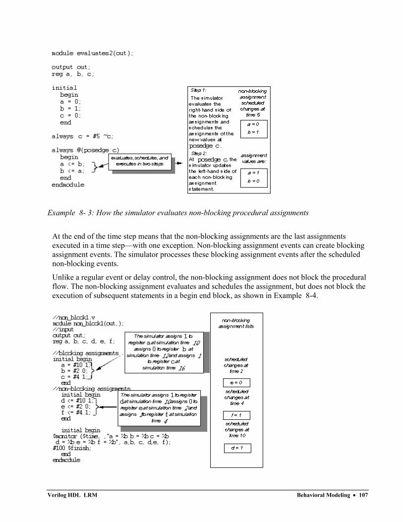
Example 8- 3: How the simulator evaluates non-blocking procedural assignments
At the end of the time step means that the non-blocking assignments are the last assignments executed in a time step—with one exception. Non-blocking assignment events can create blocking assignment events. The simulator processes these blocking assignment events after the scheduled non-blocking events.
Unlike a regular event or delay control, the non-blocking assignment does not block the procedural flow. The non-blocking assignment evaluates and schedules the assignment, but does not block the execution of subsequent statements in a begin end block, as shown in Example 8-4.
Verilog HDL LRM Behavioral Modeling • 107
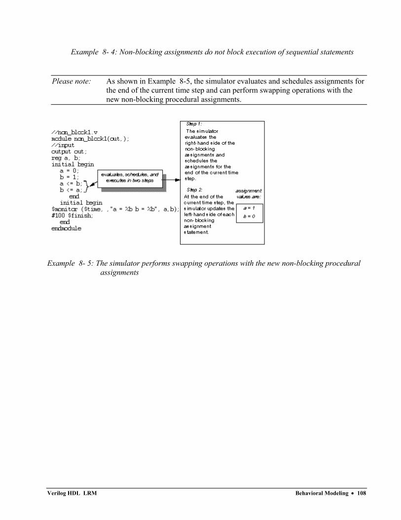
Example 8- 4: Non-blocking assignments do not block execution of sequential statements
Please note: As shown in Example 8-5, the simulator evaluates and schedules assignments for the end of the current time step and can perform swapping operations with the new non-blocking procedural assignments.
Example 8- 5: The simulator performs swapping operations with the new non-blocking procedural assignments
Verilog HDL LRM Behavioral Modeling • 108
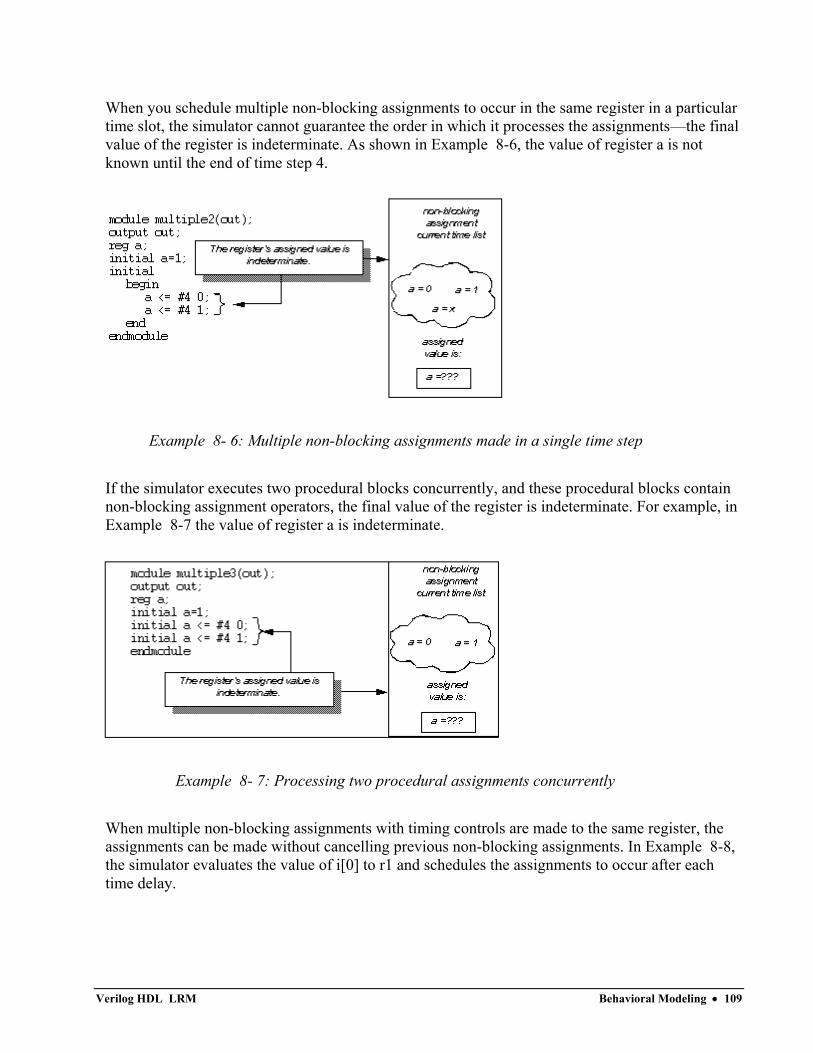
When you schedule multiple non-blocking assignments to occur in the same register in a particular time slot, the simulator cannot guarantee the order in which it processes the assignments—the final value of the register is indeterminate. As shown in Example 8-6, the value of register a is not known until the end of time step 4.
Example 8- 6: Multiple non-blocking assignments made in a single time step
If the simulator executes two procedural blocks concurrently, and these procedural blocks contain non-blocking assignment operators, the final value of the register is indeterminate. For example, in Example 8-7 the value of register a is indeterminate.
Example 8- 7: Processing two procedural assignments concurrently
When multiple non-blocking assignments with timing controls are made to the same register, the assignments can be made without cancelling previous non-blocking assignments. In Example 8-8, the simulator evaluates the value of i[0] to r1 and schedules the assignments to occur after each time delay.
Verilog HDL LRM Behavioral Modeling • 109
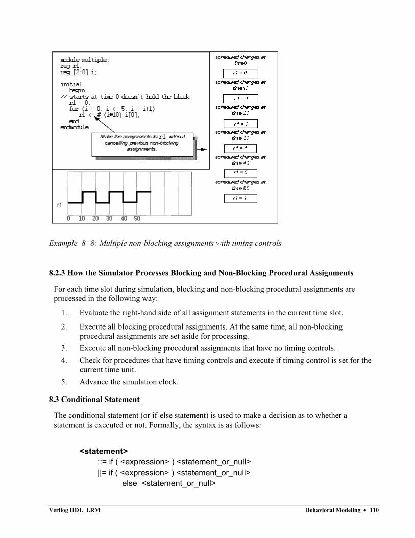
Example 8- 8: Multiple non-blocking assignments with timing controls
8.2.3 How the Simulator Processes Blocking and Non-Blocking Procedural Assignments
For each time slot during simulation, blocking and non-blocking procedural assignments are processed in the following way:
1. Evaluate the right-hand side of all assignment statements in the current time slot.
2. Execute all blocking procedural assignments. At the same time, all non-blocking procedural assignments are set aside for processing.
3. Execute all non-blocking procedural assignments that have no timing controls. 4. Check for procedures that have timing controls and execute if timing control is set for the
current time unit. 5. Advance the simulation clock.
8.3 Conditional Statement
The conditional statement (or if-else statement) is used to make a decision as to whether a statement is executed or not. Formally, the syntax is as follows:
<statement> ::= if ( <expression> ) <statement_or_null> ||= if ( <expression> ) <statement_or_null> else <statement_or_null>
Verilog HDL LRM Behavioral Modeling • 110
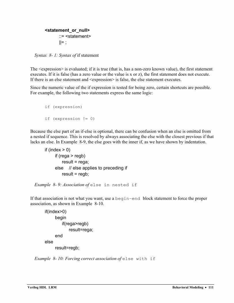
<statement_or_null> ::= <statement> ||= ;
Syntax 8- 1: Syntax of if statement
The <expression> is evaluated; if it is true (that is, has a non-zero known value), the first statement executes. If it is false (has a zero value or the value is x or z), the first statement does not execute. If there is an else statement and <expression> is false, the else statement executes.
Since the numeric value of the if expression is tested for being zero, certain shortcuts are possible. For example, the following two statements express the same logic:
if (expression)
if (expression != 0)
Because the else part of an if-else is optional, there can be confusion when an else is omitted from a nested if sequence. This is resolved by always associating the else with the closest previous if that lacks an else. In Example 8-9, the else goes with the inner if, as we have shown by indentation.
if (index > 0) if (rega > regb)
result = rega; else // else applies to preceding if
result = regb;
Example 8- 9: Association of else in nested if
If that association is not what you want, use a begin-end block statement to force the proper association, as shown in Example 8-10.
if(index>0) begin
if(rega>regb) result=rega;
end else
result=regb;
Example 8- 10: Forcing correct association of else with if
Verilog HDL LRM Behavioral Modeling • 111
Begin-end blocks left out inadvertently can change the logic behavior being expressed, as shown in Example 8-11.
if(index>0) for(scani=0;scani<index; scani=scani+1) if(memory[scani]>0) begin $display("..."); memory[scani]=0; end else/*WRONG*/ $display("error-indexiszero");
Example 8- 11: Erroneous association of else with if
The indentation in Example 8-11 shows unequivocally what you want, but the compiler does not get the message and associates the else with the inner if. This kind of bug can be very hard to find.
Notice that in Example 8-12, there is a semicolon after result = rega. This is because a <statement> follows the if, and a semicolon is an essential part of the syntax of a <statement>.
if (rega>regb) result=rega; else result=regb;
Example 8- 12: Use of semicolon in if statement
8.3.1 if-else-if Construct
The following construction occurs so often that it is worth a brief separate discussion:
if (<expression>) <statement>
else if (<expression>) <statement>
else if (<expression>) <statement>
else <statement>
Syntax 8- 2: Syntax of if-else-if construct
Verilog HDL LRM Behavioral Modeling • 112
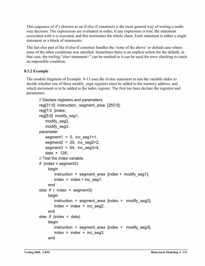
This sequence of if’s (known as an if-else-if construct) is the most general way of writing a multi-way decision. The expressions are evaluated in order; if any expression is true, the statement associated with it is executed, and this terminates the whole chain. Each statement is either a single statement or a block of statements.
The last else part of the if-else-if construct handles the ‘none of the above’ or default case where none of the other conditions was satisfied. Sometimes there is no explicit action for the default; in that case, the trailing “else<statement>” can be omitted or it can be used for error checking to catch an impossible condition.
8.3.2 Example
The module fragment of Example 8-13 uses the if-else statement to test the variable index to decide whether one of three modify_segn registers must be added to the memory address, and which increment is to be added to the index register. The first ten lines declare the registers and parameters.
// Declare registers and parameters reg[31:0] instruction, segment_area [255:0]; reg[7:0 ]index; reg[5:0] modify_seg1, modify_seg2, modify_seg3; parameter segment1 = 0, inc_seg1=1, segment2 = 20, inc_seg2=2, segment3 = 64, inc_seg3=4, data = 128; // Test the index variable if (index < segment2)
begin instruction = segment_area [index + modify_seg1]; index = index + inc_seg1;
end else if ( index < segment3)
begin instruction = segment_area [index + modify_seg2]; index = index + inc_seg2;
end else if (index < data)
begin instruction = segment_area [index + modify_seg3]; index = index + inc_seg3;
end
Verilog HDL LRM Behavioral Modeling • 113
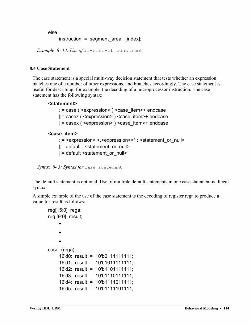
else instruction = segment_area [index];
Example 8- 13: Use of if-else-if construct
8.4 Case Statement
The case statement is a special multi-way decision statement that tests whether an expression matches one of a number of other expressions, and branches accordingly. The case statement is useful for describing, for example, the decoding of a microprocessor instruction. The case statement has the following syntax:
<statement> ::= case ( <expression> ) <case_item>+ endcase ||= casez ( <expression> ) <case_item>+ endcase ||= casex ( <expression> ) <case_item>+ endcase
<case_item> ::= <expression> <,<expression>>* : <statement_or_null> ||= default : <statement_or_null> ||= default <statement_or_null>
Syntax 8- 3: Syntax for case statement
The default statement is optional. Use of multiple default statements in one case statement is illegal syntax.
A simple example of the use of the case statement is the decoding of register rega to produce a value for result as follows:
reg[15:0] rega; reg [9:0] result;
•
•
•
case (rega) 16'd0: result = 10'b0111111111; 16'd1: result = 10'b1011111111; 16'd2: result = 10'b1101111111; 16'd3: result = 10'b1110111111; 16'd4: result = 10'b1111011111; 16'd5: result = 10'b1111101111;
Verilog HDL LRM Behavioral Modeling • 114
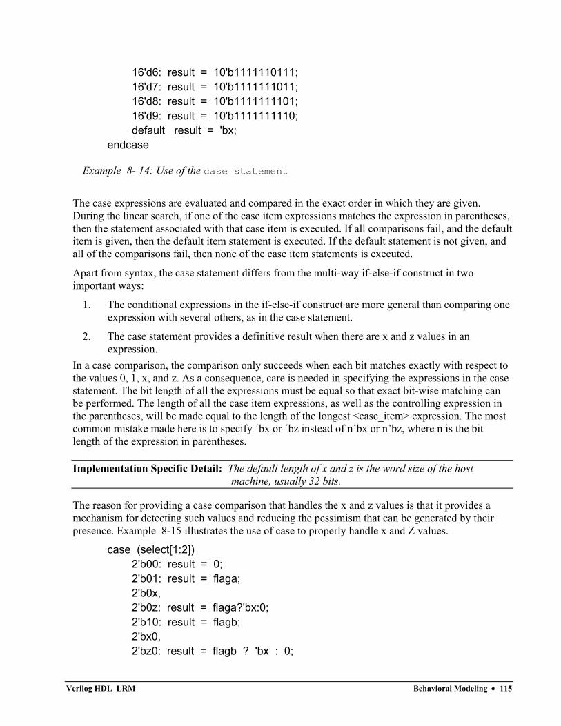
16'd6: result = 10'b1111110111; 16'd7: result = 10'b1111111011; 16'd8: result = 10'b1111111101; 16'd9: result = 10'b1111111110; default result = 'bx;
endcase
Example 8- 14: Use of the case statement
The case expressions are evaluated and compared in the exact order in which they are given. During the linear search, if one of the case item expressions matches the expression in parentheses, then the statement associated with that case item is executed. If all comparisons fail, and the default item is given, then the default item statement is executed. If the default statement is not given, and all of the comparisons fail, then none of the case item statements is executed.
Apart from syntax, the case statement differs from the multi-way if-else-if construct in two important ways:
1. The conditional expressions in the if-else-if construct are more general than comparing one expression with several others, as in the case statement.
2. The case statement provides a definitive result when there are x and z values in an expression.
In a case comparison, the comparison only succeeds when each bit matches exactly with respect to the values 0, 1, x, and z. As a consequence, care is needed in specifying the expressions in the case statement. The bit length of all the expressions must be equal so that exact bit-wise matching can be performed. The length of all the case item expressions, as well as the controlling expression in the parentheses, will be made equal to the length of the longest <case_item> expression. The most common mistake made here is to specify ´bx or ´bz instead of n’bx or n’bz, where n is the bit length of the expression in parentheses.
Implementation Specific Detail: The default length of x and z is the word size of the host machine, usually 32 bits.
The reason for providing a case comparison that handles the x and z values is that it provides a mechanism for detecting such values and reducing the pessimism that can be generated by their presence. Example 8-15 illustrates the use of case to properly handle x and Z values.
case (select[1:2]) 2'b00: result = 0; 2'b01: result = flaga; 2'b0x, 2'b0z: result = flaga?'bx:0; 2'b10: result = flagb; 2'bx0, 2'bz0: result = flagb ? 'bx : 0;
Verilog HDL LRM Behavioral Modeling • 115
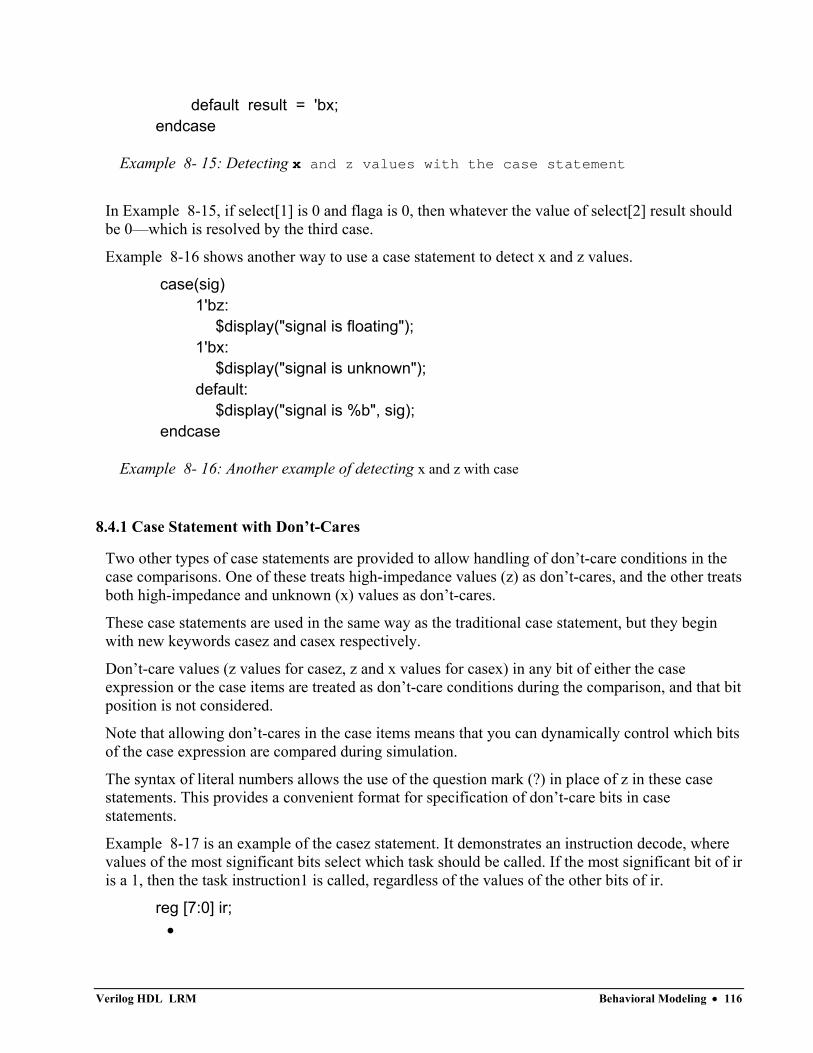
default result = 'bx; endcase
Example 8- 15: Detecting x and z values with the case statement
In Example 8-15, if select[1] is 0 and flaga is 0, then whatever the value of select[2] result should be 0—which is resolved by the third case.
Example 8-16 shows another way to use a case statement to detect x and z values.
case(sig) 1'bz: $display("signal is floating"); 1'bx: $display("signal is unknown"); default: $display("signal is %b", sig);
endcase
Example 8- 16: Another example of detecting x and z with case
8.4.1 Case Statement with Don’t-Cares
Two other types of case statements are provided to allow handling of don’t-care conditions in the case comparisons. One of these treats high-impedance values (z) as don’t-cares, and the other treats both high-impedance and unknown (x) values as don’t-cares.
These case statements are used in the same way as the traditional case statement, but they begin with new keywords casez and casex respectively.
Don’t-care values (z values for casez, z and x values for casex) in any bit of either the case expression or the case items are treated as don’t-care conditions during the comparison, and that bit position is not considered.
Note that allowing don’t-cares in the case items means that you can dynamically control which bits of the case expression are compared during simulation.
The syntax of literal numbers allows the use of the question mark (?) in place of z in these case statements. This provides a convenient format for specification of don’t-care bits in case statements.
Example 8-17 is an example of the casez statement. It demonstrates an instruction decode, where values of the most significant bits select which task should be called. If the most significant bit of ir is a 1, then the task instruction1 is called, regardless of the values of the other bits of ir.
reg [7:0] ir; •
Verilog HDL LRM Behavioral Modeling • 116
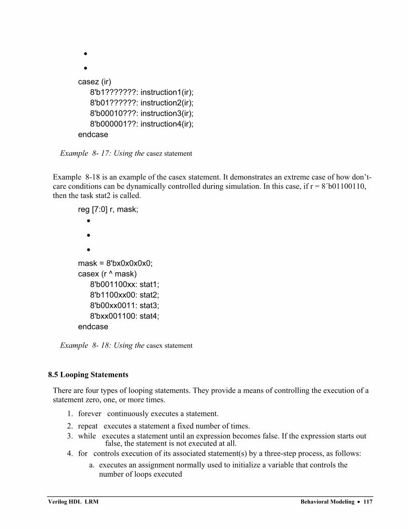
•
•
casez (ir) 8'b1???????: instruction1(ir); 8'b01??????: instruction2(ir); 8'b00010???: instruction3(ir); 8'b000001??: instruction4(ir); endcase
Example 8- 17: Using the casez statement
Example 8-18 is an example of the casex statement. It demonstrates an extreme case of how don’t-care conditions can be dynamically controlled during simulation. In this case, if r = 8´b01100110, then the task stat2 is called.
reg [7:0] r, mask; •
•
•
mask = 8'bx0x0x0x0; casex (r ^ mask) 8'b001100xx: stat1; 8'b1100xx00: stat2; 8'b00xx0011: stat3; 8'bxx001100: stat4; endcase
Example 8- 18: Using the casex statement
8.5 Looping Statements
There are four types of looping statements. They provide a means of controlling the execution of a statement zero, one, or more times.
1. forever continuously executes a statement. 2. repeat executes a statement a fixed number of times. 3. while executes a statement until an expression becomes false. If the expression starts out
false, the statement is not executed at all. 4. for controls execution of its associated statement(s) by a three-step process, as follows:
a. executes an assignment normally used to initialize a variable that controls the number of loops executed
Verilog HDL LRM Behavioral Modeling • 117
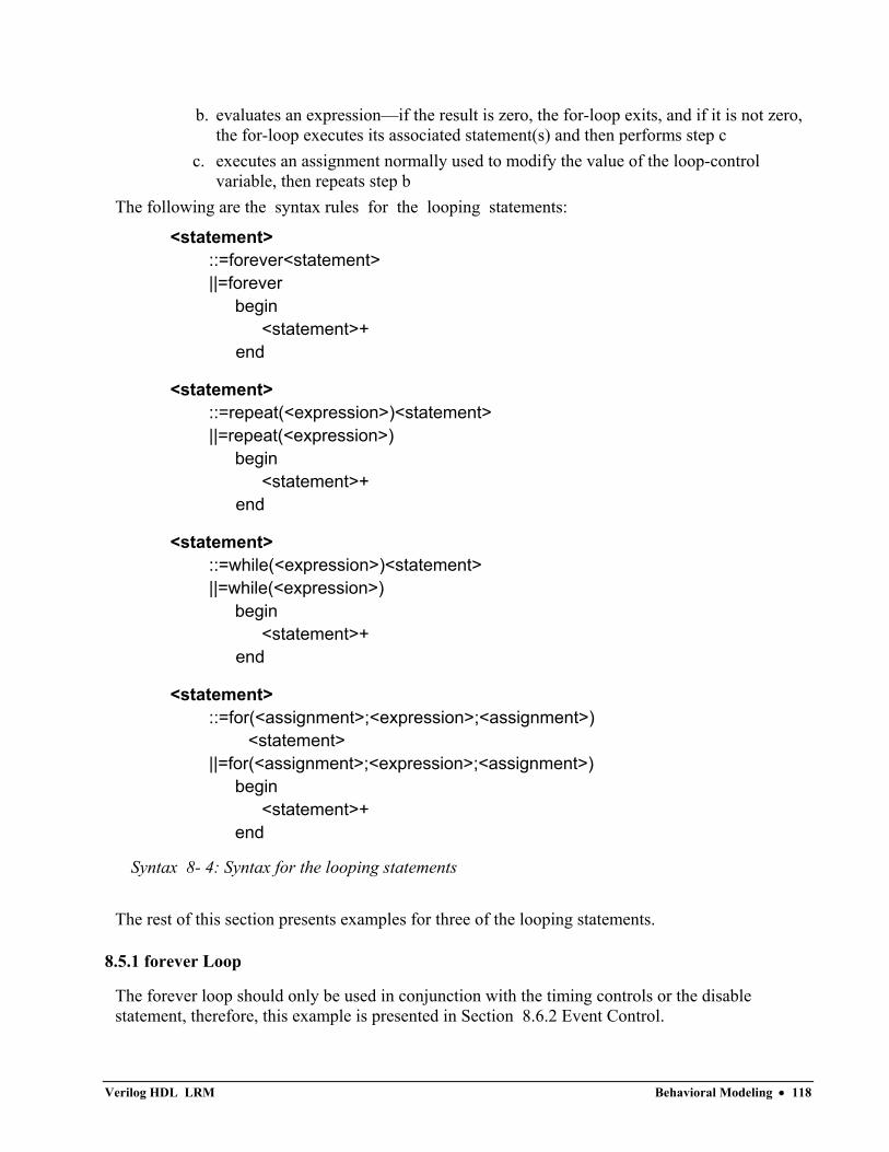
b. evaluates an expression—if the result is zero, the for-loop exits, and if it is not zero, the for-loop executes its associated statement(s) and then performs step c
c. executes an assignment normally used to modify the value of the loop-control variable, then repeats step b
The following are the syntax rules for the looping statements:
<statement> ::=forever<statement> ||=forever
begin <statement>+ end
<statement> ::=repeat(<expression>)<statement> ||=repeat(<expression>)
begin <statement>+ end
<statement> ::=while(<expression>)<statement> ||=while(<expression>)
begin <statement>+ end
<statement> ::=for(<assignment>;<expression>;<assignment>)
<statement> ||=for(<assignment>;<expression>;<assignment>)
begin <statement>+ end
Syntax 8- 4: Syntax for the looping statements
The rest of this section presents examples for three of the looping statements.
8.5.1 forever Loop
The forever loop should only be used in conjunction with the timing controls or the disable statement, therefore, this example is presented in Section 8.6.2 Event Control.
Verilog HDL LRM Behavioral Modeling • 118
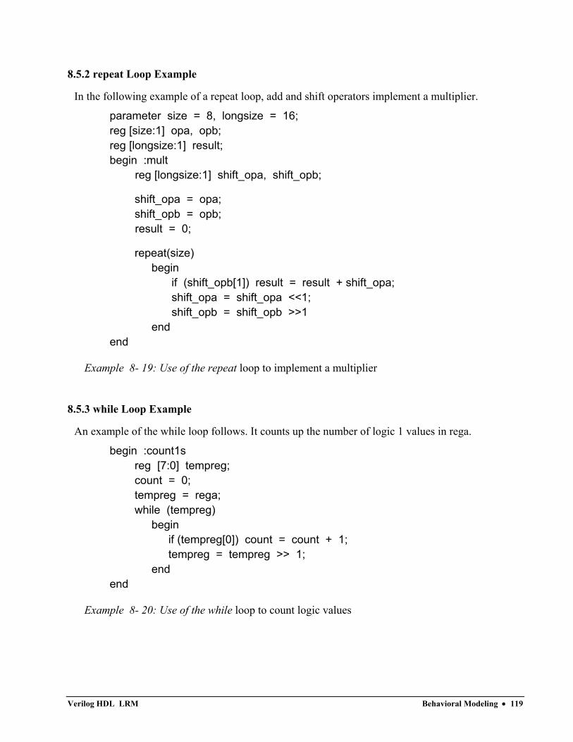
8.5.2 repeat Loop Example
In the following example of a repeat loop, add and shift operators implement a multiplier.
parameter size = 8, longsize = 16; reg [size:1] opa, opb; reg [longsize:1] result; begin :mult
reg [longsize:1] shift_opa, shift_opb;
shift_opa = opa; shift_opb = opb; result = 0;
repeat(size) begin
if (shift_opb[1]) result = result + shift_opa; shift_opa = shift_opa <<1; shift_opb = shift_opb >>1
end end
Example 8- 19: Use of the repeat loop to implement a multiplier
8.5.3 while Loop Example
An example of the while loop follows. It counts up the number of logic 1 values in rega.
begin :count1s reg [7:0] tempreg; count = 0; tempreg = rega; while (tempreg)
begin if (tempreg[0]) count = count + 1; tempreg = tempreg >> 1;
end end
Example 8- 20: Use of the while loop to count logic values
Verilog HDL LRM Behavioral Modeling • 119
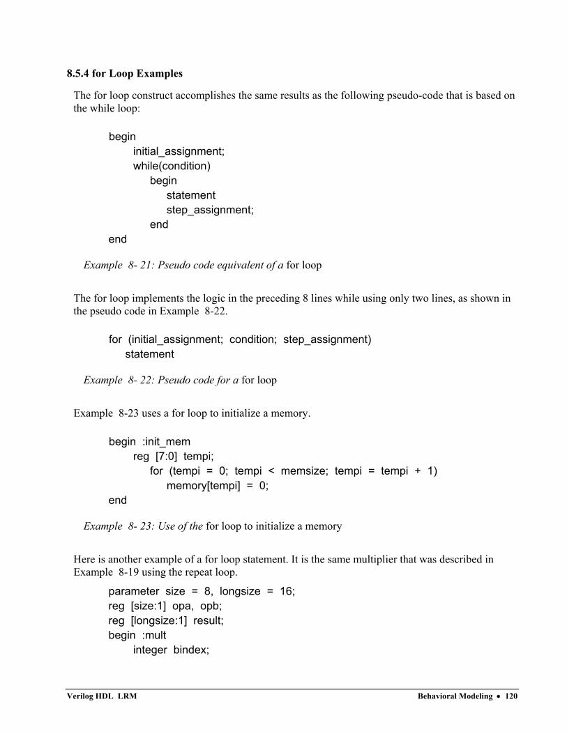
8.5.4 for Loop Examples
The for loop construct accomplishes the same results as the following pseudo-code that is based on the while loop:
begin initial_assignment; while(condition)
begin statement step_assignment;
end end
Example 8- 21: Pseudo code equivalent of a for loop
The for loop implements the logic in the preceding 8 lines while using only two lines, as shown in the pseudo code in Example 8-22.
for (initial_assignment; condition; step_assignment) statement
Example 8- 22: Pseudo code for a for loop
Example 8-23 uses a for loop to initialize a memory.
begin :init_mem reg [7:0] tempi;
for (tempi = 0; tempi < memsize; tempi = tempi + 1) memory[tempi] = 0;
end
Example 8- 23: Use of the for loop to initialize a memory
Here is another example of a for loop statement. It is the same multiplier that was described in Example 8-19 using the repeat loop.
parameter size = 8, longsize = 16; reg [size:1] opa, opb; reg [longsize:1] result; begin :mult
integer bindex;
Verilog HDL LRM Behavioral Modeling • 120
result = 0; for (bindex = 1; bindex <= size; bindex = bindex + 1)
if (opb[bindex]) result = result + (opa << (bindex-1));
end
Example 8- 24: Use of the for loop to implement a multiplier
Note that the for loop statement can be more general than the normal arithmetic progression of an index variable, as in Example 8-25. This is another way of counting the number of logic 1 values in rega (see Example 8-20).
begin :count1s reg [7:0] tempreg; count = 0; for (tempreg = rega; tempreg; tempreg = tempreg >>1)
if (tempreg[0]) count = count + 1; end
Example 8- 25: Use of the for loop to count logic values
8.6 Procedural Timing Controls
The Verilog language provides two types of explicit timing control over when in simulation time procedural statements are to occur. The first type is a delay control in which an expression specifies the time duration between initially encountering the statement and when the statement actually executes. The delay expression can be a dynamic function of the state of the circuit, but is usually a simple number that separates statement executions in time. The delay control is an important feature when specifying stimulus waveform descriptions. It is described in Sections 8.6.1, and 8.6.6.
The second type of timing control is the event expression, which allows statement execution to wait for the occurrence of some simulation event occurring in a procedure executing concurrently with this procedure. A simulation event can be a change of value on a net or register (an implicit event), or the occurrence of an explicitly named event that is triggered from other procedures (an explicit event). Most often, an event control is a positive or negative edge on a clock signal. Sections 8.6.2 through 8.6.6 discuss event control.
A general principle of the Verilog language is that “where you do not see a timing control, then simulation time does not advance.” Though we are talking here of procedural timing controls, note that gate and net delays also advance simulation time. The procedural statements encountered so far all execute in zero time. Simulation time can only progress by one of the following three methods:
• a delay control, which is introduced by the number symbol (#)
Verilog HDL LRM Behavioral Modeling • 121
• an event control, which is introduced by the at symbol (@)
• the wait statement, which operates like a combination of the event control and the while loop
The next subsections discuss these three methods.
8.6.1 Delay Control
The execution of a procedural statement can be delay-controlled by using the following syntax:
<statement> ::= <delay_control> <statement_or_null>
<delay_control> ::= # <NUMBER> ||= # <identifier> ||= # ( <mintypmax_expression> )
Syntax 8- 5: Syntax for delay_control
The following example delays the execution of the assignment by 10 time units:
#10 rega = regb;
The next three examples provide an expression following the number sign (#). Execution of the assignment delays by the amount of simulation time specified by the value of the expression.
#d rega = regb; // d is defined as a parameter
#((d+e)/2) rega = regb; // delay is the average of d and e
#regr regr = regr + 1; // delay is the value in regr
8.6.2 Event Control
The execution of a procedural statement can be synchronized with a value change on a net or register, or the occurrence of a declared event, by using the following event control syntax:
<statement> ::= <event_control> <statement_or_null>
<event_control> ::= @ <identifier> ||= @ ( <event_expression> )
<event_expression>
Verilog HDL LRM Behavioral Modeling • 122
::= <expression> ||= posedge <SCALAR_EVENT_EXPRESSION> ||= negedge <SCALAR_EVENT_EXPRESSION> ||= <event_expression> <or <event_expression>>*
<SCALAR_EVENT_EXPRESSION> is an expression that resolves to a one bit value.
Syntax 8- 6: Syntax for event_control
Value changes on nets and registers can be used as events to trigger the execution of a statement. This is known as detecting an implicit event. See item 1 in Example 8-26 for a syntax example of a wait for an implicit event. Verilog syntax also allows you to detect change based on the direction of the change—that is, toward the value 1 (posedge) or toward the value 0 (negedge). The behavior of posedge and negedge for unknown expression values is as follows:
• a negedge is detected on the transition from 1 to unknown and from unknown to 0
• a posedge is detected on the transition from 0 to unknown and from unknown to 1
Items 2 and 3 in Example 8-26 show illustrations of edge controlled statements.
Item 1 @ rrega = regb; //controlled by any value changes in the register rrega
Item 2 @ (posedge clock) rega = regb; //controlled by positive edge on clock
Item 3 forever @ (negedge clock) rega = regb; // controlled by negative edge
Example 8- 26: Event controlled statements
8.6.3 Named Events
Verilog also provides syntax to name an event and then to trigger the occurrence of that event. A model can then use an event expression to wait for the triggering of this explicit event. Named events can be made to occur from a procedure. This allows control over the enabling of multiple actions in other procedures. Named events and event control give a powerful and efficient means of describing the communication between, and synchronization of, two or more concurrently active processes. A basic example of this is a small waveform clock generator that synchronizes control of a synchronous circuit by signalling the occurrence of an explicit event periodically while the circuit waits for the event to occur.
An event name must be declared explicitly before it is used. The following is the syntax for declaring events.
<event_declaration>
Verilog HDL LRM Behavioral Modeling • 123
::= event <name_of_event> <,<name_of_event>>* ;
<name_of_event> ::= <IDENTIFIER> - the name of an explicit event
Syntax 8- 7: Syntax for event_declaration
Note that an event does not hold any data. The following are the characteristics of a Verilog event:
• it can be made to occur at any particular time
• it has no time duration
• its occurrence can be recognized by using the <event_control> syntax described in Section 8.6.2
The power of the explicit event is that it can represent any general happening. For example, it can represent a positive edge of a clock signal, or it can represent a microprocessor transferring data down a serial communications channel. A declared event is made to occur by the activation of an event triggering statement of the following syntax:
-> <name_of_event> ;
An event controlled statement (for example, @trig rega = regb;) causes simulation of its containing procedure to wait until some other procedure executes the appropriate event triggering statement (for this example, ->trig).
8.6.4 Event OR Construct
The ORing of any number of events can be expressed such that the occurrence of any one will trigger the execution of the statement. The next two examples show the ORing of two and three events respectively.
@(trig or enable) rega = regb; // controlled by trig or enable
@(posedge clock_a or posedge clock_b or trig) rega = regb;
8.6.5 Level-Sensitive Event Control
The execution of a statement can also be delayed until a condition becomes true. This is accomplished using the wait statement, which is a special form of event control. The nature of the wait statement is level-sensitive, as opposed to basic event control (specified by the @ character), which is edge-sensitive. The wait statement checks a condition, and, if it is false, causes the procedure to pause until that condition becomes true before continuing. The wait statement has the following form:
wait(condition_expression) statement
Verilog HDL LRM Behavioral Modeling • 124
Example 8-27 shows the use of the wait statement to accomplish level-sensitive event control.
begin wait(!enable) #10 a = b; #10 c = d; end
Example 8- 27: Use of wait statement
If the value of enable is one when the block is entered, the wait statement delays the evaluation of the next statement (#10 a = b;) until the value of enable changes to zero. If enable is already zero when the begin-end block is entered, then the next statement is evaluated immediately and no delay occurs.
8.6.6 Intra-Assignment Timing Controls
The delay and event control constructs previously described precede a statement and delay its execution. The intra-assignment delay and event controls are contained within an assignment statement and modify the flow of activity in a slightly different way.
Encountering an intra-assignment delay or event control delays the assignment just as a regular delay or event control does, but the right-hand-side expression is evaluated before the delay, instead of after the delay. This allows data swap and data shift operations to be described without the need for temporary variables. This section describes the purpose of intra-assignment timing controls and the repeat timing control that can be used in intra-assignment delays.
Figure 8-1 illustrates the philosophy of intra-assignment timing controls by showing the code that could accomplish the same timing effect without using intra-assignment.
Figure 8- 1: Equivalents to intra-assignment timing controls
Verilog HDL LRM Behavioral Modeling • 125
The next three examples use the fork-join behavioral construct. All statements between the keywords fork and join execute concurrently. Section 8.7.2 Parallel Blocks describes this construct in more detail.
The following example shows a race condition that could be prevented by using intra-assignment timing control:
fork
#5 a = b;
#5 b = a;
join
The code in the example above samples the values of both a and b at the same simulation time, thereby creating a race condition. The intra-assignment form of timing control used in the example below prevents this race condition:
fork // data swap
a = #5 b;
b = #5 a;
join
Intra-assignment timing control works because the intra-assignment delay causes the values of a and b to be evaluated before the delay, and the assignments to be made after the delay. Some existing tools that implement intra-assignment timing control use temporary storage in evaluating each expression on the right-hand side.
Intra-assignment waiting for events is also effective. In the example below, the right-hand-side expressions are evaluated when the assignment statements are encountered, but the assignments are delayed until the rising edge of the clock signal.
fork // data shift
a = @(posedge clk) b;
b = @(posedge clk) c;
join
The repeat event control
The repeat event control specifies an intra-assignment delay of a specified number of occurrences of an event. This construct is convenient when events must be synchronized with counts of clock signals.
Syntax 8-8 presents the repeat event control syntax:
<repeat_event _controlled_assignment>
Verilog HDL LRM Behavioral Modeling • 126
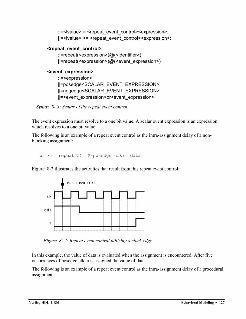
::=<lvalue> = <repeat_event_control><expression>; ||=<lvalue> <= <repeat_event_control><expression>;
<repeat_event_control> ::=repeat(<expression>)@(<identifier>) ||=repeat(<expression>)@(<event_expression>)
<event_expression> ::=<expression> ||=posedge<SCALAR_EVENT_EXPRESSION> ||=negedge<SCALAR_EVENT_EXPRESSION> ||=<event_expression>or<event_expression>
Syntax 8- 8: Syntax of the repeat event control
The event expression must resolve to a one bit value. A scalar event expression is an expression which resolves to a one bit value.
The following is an example of a repeat event control as the intra-assignment delay of a non-blocking assignment:
a <= repeat(5) @(posedge clk) data;
Figure 8-2 illustrates the activities that result from this repeat event control:
Figure 8- 2: Repeat event control utilizing a clock edge
In this example, the value of data is evaluated when the assignment is encountered. After five occurrences of posedge clk, a is assigned the value of data.
The following is an example of a repeat event control as the intra-assignment delay of a procedural assignment:
Verilog HDL LRM Behavioral Modeling • 127
a = repeat(num)@(clk)data;
In this example, the value of data is evaluated when the assignment is encountered. After the number of transitions of clk equals the value of num, a is assigned the value of data.
The following is an example of a repeat event control with expressions containing operations to specify both the number of event occurrences and the event that is counted:
a <= repeat(a+b)@(posedge phi1 or negedge phi2)data;
In the example above, the value of data is evaluated when the assignment is encountered. After the sum of the positive edges of phi1 and the negative edges of phi2 equals the sum of a and b, a is assigned the value of data.
8.7 Block Statements
The block statements are a means of grouping two or more statements together so that they act syntactically like a single statement. We have already introduced and used the sequential block statement which is delimited by the keywords begin and end. Section 8.7.1 Sequential Blocks discusses sequential blocks in more detail.
A second type of block, delimited by the keywords fork and join, is used for executing statements in parallel. A fork-join block is known as a parallel block, and enables procedures to execute concurrently through time. Section 8.7.2 Parallel Blocks discusses parallel blocks.
8.7.1 Sequential Blocks
A sequential block has the following characteristics:
• statements execute in sequence, one after another
• delay values for each statement are relative to the simulation time of the execution of the previous statement
• control passes out of the block after the last statement executes
The following is the formal syntax for a sequential block:
<seq_block> ::= begin <statement>* end ||= begin : <name_of_block>
<block_declaration>* <statement>*
end
<name_of_block> ::=<IDENTIFIER>
Verilog HDL LRM Behavioral Modeling • 128
<block_declaration> ::=<parameter_declaration> ||=<reg_declaration> ||=<integer_declaration> ||=<real_declaration>
Syntax 8- 9: Syntax for the sequential block
A sequential block enables the following two assignments to have a deterministic result:
begin
areg = breg;
creg = areg; // creg becomes the value of breg
end
Here the first assignment is performed and areg is updated before control passes to the second assignment.
Delay control can be used in a sequential block to separate the two assignments in time.
begin
areg = breg;
#10 creg = areg; // this gives a delay of 10 time
end // units between assignments
Example 8-28 shows how the combination of the sequential block and delay control can be used to specify a time-sequenced waveform.
parameter d = 50; // d declared as a parameter reg [7:0] r; // and r declared as an 8-bit register begin // a waveform controlled by sequential delay #d r = 'h35; #d r = 'hE2; #d r = 'h00; #d r = 'hF7; #d -> end_wave;// trigger the event called end_wave end
Example 8- 28: A waveform controlled by sequential delay
Example 8-29 shows three examples of sequential blocks.
Verilog HDL LRM Behavioral Modeling • 129
Example 8- 29: Three examples of sequential blocks
8.7.2 Parallel Blocks
A parallel block has the following characteristics:
• statements execute concurrently
• delay values for each statement are relative to the simulation time when control enters the block
• delay control is used to provide time-ordering for assignments
• control passes out of the block when the last time-ordered statement executes or a disable statement executes
Syntax 8-10 gives the formal syntax for a parallel block.
<par_block> ::= fork <statement>* join ||= fork : <name_of_block
<block_declaration>* <statement>*
join
<name_of_block> ::=<IDENTIFIER>
<block_declaration> ::=<parameter_declaration> ||=<reg_declaration> ||=<integer_declaration> ||=<real_declaration>
Verilog HDL LRM Behavioral Modeling • 130
||=<time_declaration> ||=<event_declaration>
Syntax 8- 10: Syntax for the parallel block
Example 8-30 codes the waveform description shown in Example 8-28 by using a parallel block instead of a sequential block. The waveform produced on the register is exactly the same for both implementations.
fork #50 r = 'h35; #100 r = 'hE2; #150 r = 'h00; #200 r = 'hF7; #250 -> end_wave; join
Example 8- 30: Use of the fork-join construct
8.7.3 Block Names
Note that blocks can be named by adding: name_of_block after the keywords begin or fork. The naming of blocks serves several purposes:
• It allows local variables to be declared for the block.
• It allows the block to be referenced in statements like the disable statement (as discussed in Chapter 10.0 Disabling Blocks and Tasks Overview).
• In the Verilog language, all variables are static—that is, a unique location exists for all variables and leaving or entering blocks does not affect the values stored in them.
Thus, block names give a means of uniquely identifying all variables at any simulation time.
8.7.4 Start and Finish Times
Both forms of blocks have the notion of a start and finish time. For sequential blocks, the start time is when the first statement is executed, and the finish time is when the last statement has finished. For parallel blocks, the start time is the same for all the statements, and the finish time is when the last time-ordered statement has finished executing. When blocks are embedded within each other, the timing of when a block starts and finishes is important. Execution does not continue to the statement following a block until the block’s finish time has been reached—that is, until the block has completely finished executing.
Moreover, the timing controls in a fork-join block do not have to be given sequentially in time. Example 8-31 shows the statements from Example 8-30 written in the reverse order and still producing the same waveform.
Verilog HDL LRM Behavioral Modeling • 131
fork #250 -> end_wave; #200 r = 'hF7; #150 r = 'h00; #100 r = 'hE2; #50 r = 'h35; join
Example 8- 31: Timing controls in a parallel block
Sequential and parallel blocks can be embedded within each other allowing complex control structures to be expressed easily and with a high degree of structure.
One simple example of this is when an assignment is to be made after two separate events have occurred. This is known as the ‘joining’ of events.
begin fork
@Aevent; @Bevent;
join areg=breg;
end
Example 8- 32: The joining of events
Note that the two events can occur in any order (or even at the same time) and the fork-join block will complete and the assignment will be made. In contrast to this, if the fork-join block was a begin-end block and the Bevent occurred before the Aevent, then the block would be deadlocked waiting for the Bevent.
Example 8-33 shows two sequential blocks, each of which will execute when its controlling event occurs. Because the wait statements are within a fork-join block, they execute in parallel and the sequential blocks can therefore also execute in parallel.
fork @enable_a
begin #tawa=0; #tawa=1; #tawa=0;
end @enable_b
Verilog HDL LRM Behavioral Modeling • 132
begin #tbwb=1; #tbwb=0; #tbwb=1;
end join
Example 8- 33: Enabling sequential blocks to execute in parallel
8.8 Structured Procedures
All procedures in Verilog are specified within one of the following four statements:
initial statement
• always statement
• task
• function
The initial and always statements are enabled at the beginning of simulation. The initial statement executes only once and its activity dies when the statement has finished. In contrast, the always statement executes repeatedly. Its activity dies only when the simulation is terminated. There is no limit to the number of initial and always blocks that can be defined in a module.
Tasks and functions are procedures that are enabled from one or more places in other procedures. Tasks and functions are covered in detail in Chapter 9.
8.8.1 initial Statement
The syntax for the initial statement is as follows:
<initial_statement> ::=initial<statement>
Syntax 8- 11: Syntax for <initial_statement>
Example 8-34 illustrates use of the initial statement for initialization of variables at the start of simulation.
initial begin
areg = 0; // initialize a register for (index = 0; index < size; index = index+1)
memory[index] = 0; // initialize a memory word
Verilog HDL LRM Behavioral Modeling • 133
end
Example 8- 34: Use of initial statement
Another typical usage of the initial statement is specification of waveform descriptions that execute once to provide stimulus to the main part of the circuit being simulated. Example 8-35 illustrates this usage.
initial begin
inputs = 'b000000; // initialize at time zero #10 inputs = 'b011001; // first pattern #10 inputs = 'b011011; // second pattern #10 inputs = 'b011000; // third pattern #10 inputs = 'b001000; // last pattern
end
Example 8- 35: Another use for initial statement
8.8.2 always Statement
The always statement repeats continuously throughout the whole simulation run. Syntax 8-12 gives the syntax for the always statement.
<always_statement> ::= always <statement>
Syntax 8- 12: Syntax for always_statement
The always statement, because of its looping nature, is only useful when used in conjunction with some form of timing control. If an always statement provides no means for time to advance, the always statement creates a simulation deadlock condition. The following code, for example, creates an infinite zero-delay loop.
always areg = ~areg;
Providing a timing control to the above code creates a potentially useful description—as in the following example:
always #half_period areg = ~areg;
Verilog HDL LRM Behavioral Modeling • 134
8.8.3 Examples
We have now introduced enough statement types for some complete and more practical examples to be given. These examples are given as complete descriptions enclosed in modules—such that they can be simulated and the results observed.
Example 8-36 is that of a simple traffic light sequencer described with its own clock generator.
module traffic_lights; reg clock, red, amber, green; parameter
on = 1, off = 0, red_tics = 350, amber_tics = 30, green_tics = 200;
// the sequence to control the lights always
begin red = on; amber = off; green = off; repeat (red_tics) @(posedge clock); red = off; green = on; repeat (green_tics) @(posedge clock); green = off; amber = on; repeat (amber_tics) @(posedge clock);
end // waveform for the clock always
begin #100 clock = 0; #100 clock = 1;
end // simulate for 10 changes on the red light initial
begin
Verilog HDL LRM Behavioral Modeling • 135
repeat (10) @ red; $finish;
end // display the time and changes made to the lights always
@ ( red or amber or green ) $display ("%d red=%b amber=%b green=%b", $time, red, amber, green);
endmodule
Example 8- 36: Behavioral model of traffic light sequencer
Example 8-37 shows a use of variable delays. The module has a clock input and produces two synchronized clock outputs. Each output clock has equal mark and space times, is out of phase from the other by 45 degrees, and has a period half that of the input clock. Note that the clock generation is independent of the simulation time unit, except as it affects the accuracy of the divide operation on the input clock period.
module synch_clocks; reg
clock, phase1, phase2;
time clock_time; initial clock_time = 0; always @ (posedge clock)
begin :phase_gen timed; //a local declaration is possible //because the block is named d = ($time - clock_time) / 8; clock_time = $time; phase1 = 0; #d phase2 = 1; #d phase1 = 1; #d phase2 = 0; #d phase1 = 0; #d phase2 = 1; #d phase1 = 1; #d phase2 = 0;
end // setup a clock waveform, finish time,
Verilog HDL LRM Behavioral Modeling • 136
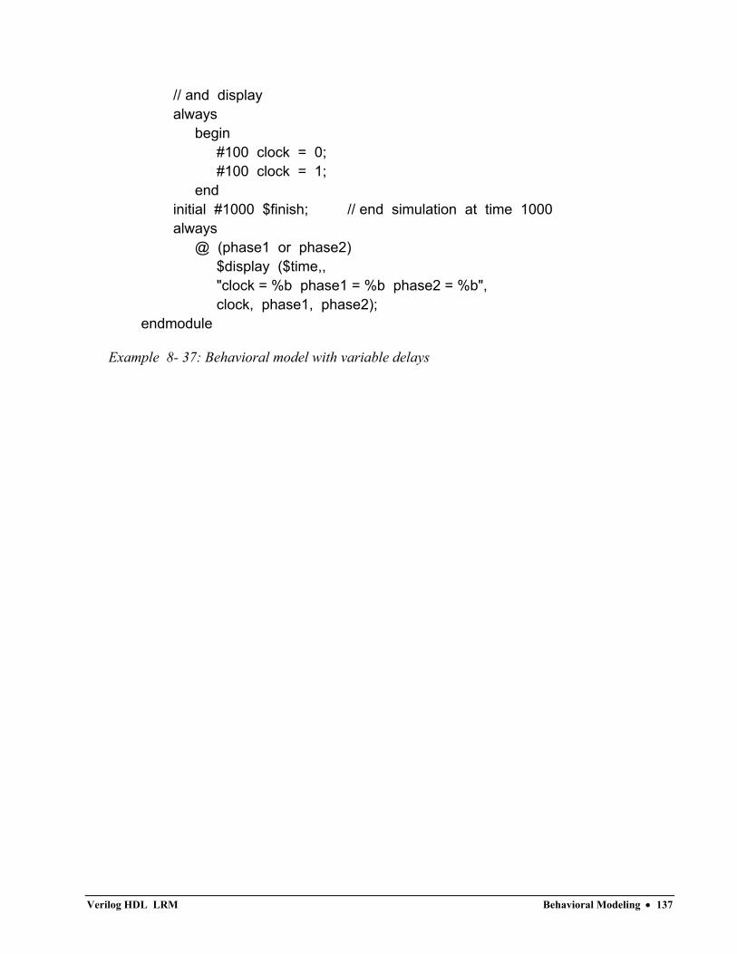
// and display always
begin #100 clock = 0; #100 clock = 1;
end initial #1000 $finish; // end simulation at time 1000 always
@ (phase1 or phase2) $display ($time,, "clock = %b phase1 = %b phase2 = %b", clock, phase1, phase2);
endmodule
Example 8- 37: Behavioral model with variable delays
Verilog HDL LRM Behavioral Modeling • 137
Tasks and Functions
9.0 Tasks and Functions Overview
Tasks and functions provide the ability to execute common procedures from several different places in a description. They also provide a means of breaking up large procedures into smaller ones to make it easier to read and debug the source descriptions. Input, output, and inout argument values can be passed into and out of both tasks and functions. The next section discusses the differences between tasks and functions. Subsequent sections describe how to define and invoke tasks and functions and present examples of each.
9.1 Distinctions between Tasks and Functions
The following rules distinguish tasks from functions:
• A function must execute in one simulation time unit; a task can contain time-controlling statements.
• A function cannot enable a task; a task can enable other tasks and functions.
• A function must have at least one input argument; a task can have zero or more arguments of any type.
• A function returns a single value; a task does not return a value.
The purpose of a function is to respond to an input value by returning a single value. A task can support multiple goals and can calculate multiple result values. However, only the output or inout arguments pass result values back from the invocation of a task. A Verilog model uses a function as an operand in an expression; the value of that operand is the value returned by the function.
For example, you could define either a task or a function to switch bytes in a 16-bit word. The task would return the switched word in an output argument, so the source code to enable a task called switch_bytes could look like the following example:
switch_bytes (old_word, new_word);
The task switch_bytes would take the bytes in old_word, reverse their order, and place the reversed bytes in new_word. A word-switching function would return the switched word directly. Thus, the function call for the function switch_bytes might look like the following example:
new_word = switch_bytes (old_word);
9.2 Tasks and Task Enabling
A task is enabled from a statement that defines the argument values to be passed to the task and the variables that will receive the results. Control is passed back to the enabling process after the task has completed. Thus, if a task has timing controls inside it, then the time of enabling can be different from the time at which control is returned. A task can enable other tasks, which in turn
Verilog HDL LRM Tasks and Functions • 138
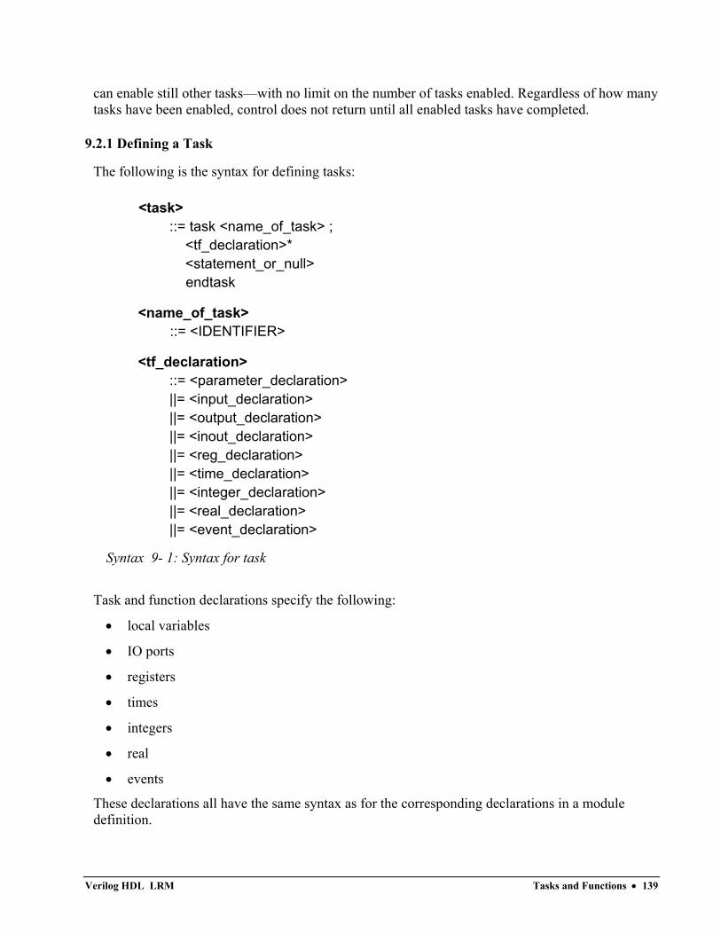
can enable still other tasks—with no limit on the number of tasks enabled. Regardless of how many tasks have been enabled, control does not return until all enabled tasks have completed.
9.2.1 Defining a Task
The following is the syntax for defining tasks:
<task> ::= task <name_of_task> ; <tf_declaration>* <statement_or_null> endtask
<name_of_task> ::= <IDENTIFIER>
<tf_declaration> ::= <parameter_declaration> ||= <input_declaration> ||= <output_declaration> ||= <inout_declaration> ||= <reg_declaration> ||= <time_declaration> ||= <integer_declaration> ||= <real_declaration> ||= <event_declaration>
Syntax 9- 1: Syntax for task
Task and function declarations specify the following:
• local variables
• IO ports
• registers
• times
• integers
• real
• events
These declarations all have the same syntax as for the corresponding declarations in a module definition.
Verilog HDL LRM Tasks and Functions • 139
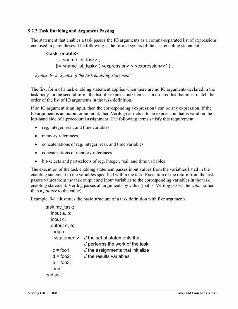
9.2.2 Task Enabling and Argument Passing
The statement that enables a task passes the IO arguments as a comma-separated list of expressions enclosed in parentheses. The following is the formal syntax of the task enabling statement:
<task_enable> ::= <name_of_task> ; ||= <name_of_task> ( <expression> <,<expression>>* ) ;
Syntax 9- 2: Syntax of the task enabling statement
The first form of a task enabling statement applies when there are no IO arguments declared in the task body. In the second form, the list of <expression> items is an ordered list that must match the order of the list of IO arguments in the task definition.
If an IO argument is an input, then the corresponding <expression> can be any expression. If the IO argument is an output or an inout, then Verilog restricts it to an expression that is valid on the left-hand side of a procedural assignment. The following items satisfy this requirement:
• reg, integer, real, and time variables
• memory references
• concatenations of reg, integer, real, and time variables
• concatenations of memory references
• bit-selects and part-selects of reg, integer, real, and time variables
The execution of the task enabling statement passes input values from the variables listed in the enabling statement to the variables specified within the task. Execution of the return from the task passes values from the task output and inout variables to the corresponding variables in the task enabling statement. Verilog passes all arguments by value (that is, Verilog passes the value rather than a pointer to the value).
Example 9-1 illustrates the basic structure of a task definition with five arguments.
task my_task; input a, b; inout c; output d, e; begin <statement> // the set of statements that // performs the work of the task c = foo1; // the assignments that initialize d = foo2; // the results variables e = foo3; end endtask
Verilog HDL LRM Tasks and Functions • 140
Example 9- 1: Task definition with arguments
The following statement enables the task in Example 9-1:
my_task (v, w, x, y, z);
The calling arguments (v, w, x, y, z) correspond to the IO arguments (a, b, c, d, e) defined by the task. At task enabling time, the input and inout arguments (a, b, and c) receive the values passed in v, w, and x. A tool processing the HDL source code performs this assignment. Thus, execution of the task enabling call effectively causes the following assignments:
a = v; b = w; c = x;
As part of the processing of the task, the task definition for my_task must place the computed results values into c, d, and e. When the task completes, the processing software performs the following assignments to return the computed values to the calling process:
x = c; y = d; z = e;
9.2.3 Task Example
Example 9-2 illustrates the use of tasks by redescribing the traffic light sequencer that was introduced in Chapter 8.
module traffic_lights; reg clock, red, amber, green; parameter on = 1, off = 0, red_tics = 350, amber_tics = 30, green_tics = 200; // initialize colors initial red = off; initial amber = off; initial green = off; // sequence to control the lights always begin red = on; // turn red light on light(red, red_tics); // and wait. green = on; // turn green light on light(green, green_tics); // and wait. amber = on; // turn amber light on light(amber, amber_tics); // and wait. end
Verilog HDL LRM Tasks and Functions • 141
// task to wait for 'tics' positive edge clocks // before turning 'color' light off task light; output color; input [31:0] tics; begin repeat (tics) @(posedge clock); color = off; // turn light off end endtask // waveform for the clock always begin #100 clock = 0; #100 clock = 1; end endmodule // traffic_lights
Example 9- 2: Using tasks
9.2.4 Effect of Enabling an Already Active Task
Implementation Specific Detail: Because Verilog supports concurrent procedures, and tasks can have non-zero time duration, you can write a model that invokes a task when that task is already executing (a special case of invoking a task that is already active is where a task recursively calls itself). Some tools allow multiple copies of a task to execute concurrently, but it does not copy or otherwise preserve the task arguments or local variables. Some tools use the same storage for each invocation of the task. This means that when the simulator interrupts a task to process another instance of the same task, it overwrites the argument values from the first call with the values from the second call. The user must manage what happens to the variables of a task that is invoked while it is already active.
9.3 Functions and Function Calling
The purpose of a function is to return a value that is to be used in an expression. The rest of this chapter explains how to define and use functions.
Verilog HDL LRM Tasks and Functions • 142
9.3.1 Defining a Function
To define functions, use the following syntax:
<function> ::= function <range_or_type>? <name_of_function> ; <tf_declaration>+ <statement> endfunction
<range_or_type> ::= <range> ||= integer ||= real
<name_of_function> ::= <IDENTIFIER>
<tf_declaration> ::= <parameter_declaration> ||= <input_declaration> ||= <output_declaration> ||= <inout_declaration> ||= <reg_declaration> ||= <time_declaration> ||= <integer_declaration> ||= <real_declaration> ||= <event_declaration>
Syntax 9- 3: Syntax for function
Note that the <range_or_type> item is optional. A function specified without <range_or_type> defaults to a one-bit register for the return value. If used, <range_or_type> can specify that the function’s return value is a real, an integer, or a value with a range of [n:m] bits.
Example 9-3 defines a function called getbyte, using a <range> specification.
function [7:0] getbyte; input [15:0] address; begin <statements> // code to extract low-order // byte from addressed word getbyte = result_expression; end endfunction
Verilog HDL LRM Tasks and Functions • 143
Example 9- 3: A function definition using range
9.3.2 Returning a Value from a Function
The function definition implicitly declares a register, internal to the function, with the same name as the function. This register either defaults to one bit or is the same type as the <range_or_type> specified in the function declaration. The function definition initializes the function’s return value by assigning the function result to the internal variable with the same name as the function. The following line from Example 9-3 illustrates this concept:
getbyte = result_expression;
9.3.3 Calling a Function
A function call is an operand within an expression. The operand has the following syntax:
<function_call> ::= <name_of_function> ( <expression> <,<expression>>* )
<name_of_function> ::= <identifier>
Syntax 9- 4: Syntax for function_call
The following example creates a word by concatenating the results of two calls to the function getbyte (defined in Example 9-3).
word = control ? {getbyte(msbyte), getbyte(lsbyte)} : 0;
9.3.4 Function Rules
Functions are more limited than tasks. The following four rules govern their usage:
1. A function definition cannot contain any time controlled statements—that is, any statements introduced with #, @, or wait.
2. Functions cannot enable tasks. 3. A function definition must contain at least one input argument. 4. A function definition must include an assignment of the function result value to the internal
variable that has the same name as the function.
Verilog HDL LRM Tasks and Functions • 144
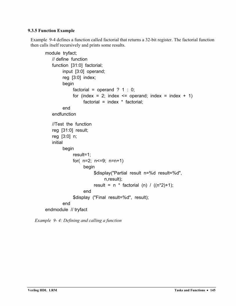
9.3.5 Function Example
Example 9-4 defines a function called factorial that returns a 32-bit register. The factorial function then calls itself recursively and prints some results.
module tryfact; // define function function [31:0] factorial; input [3:0] operand; reg [3:0] index; begin factorial = operand ? 1 : 0; for (index = 2; index <= operand; index = index + 1) factorial = index * factorial; end endfunction
//Test the function reg [31:0] result; reg [3:0] n; initial begin result=1; for( n=2; n<=9; n=n+1) begin $display("Partial result n=%d result=%d", n,result); result = n * factorial (n) / ((n*2)+1); end $display ("Final result=%d", result); end endmodule // tryfact
Example 9- 4: Defining and calling a function
Verilog HDL LRM Tasks and Functions • 145
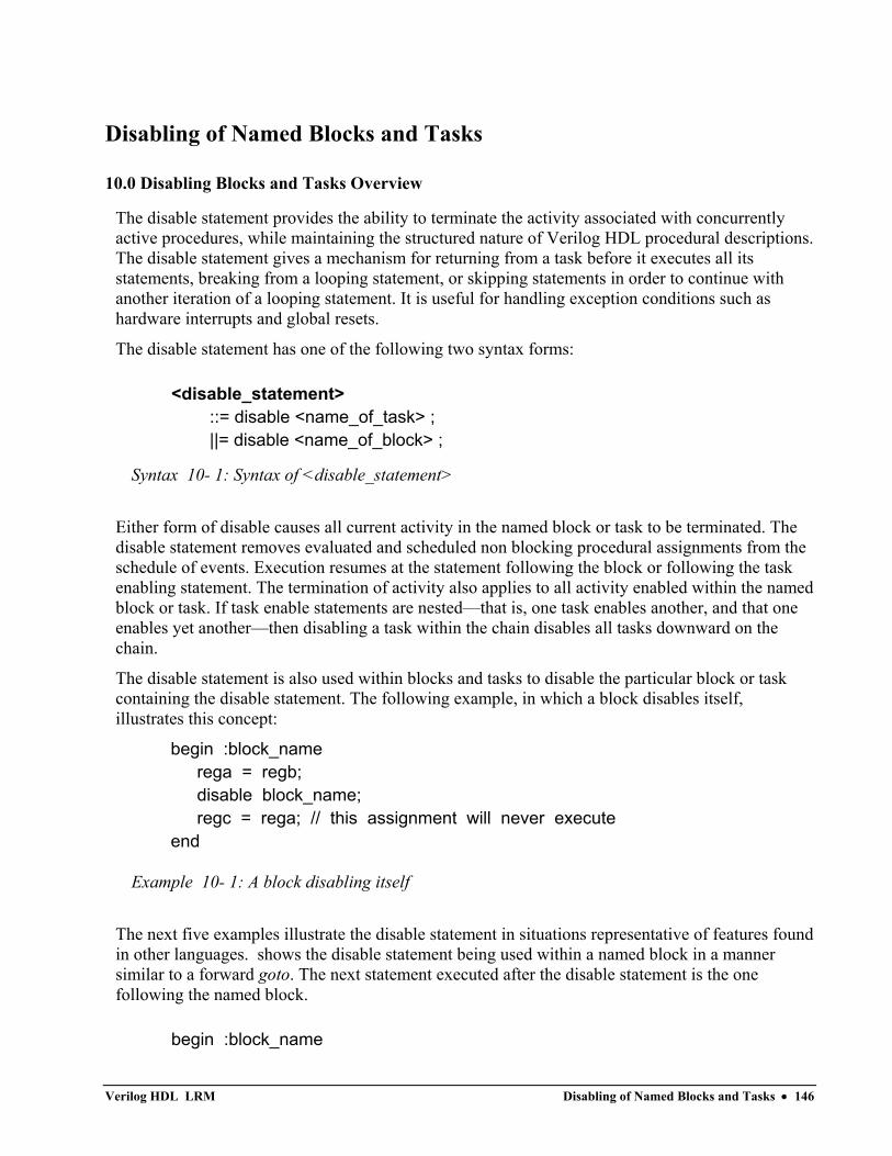
Disabling of Named Blocks and Tasks
10.0 Disabling Blocks and Tasks Overview
The disable statement provides the ability to terminate the activity associated with concurrently active procedures, while maintaining the structured nature of Verilog HDL procedural descriptions. The disable statement gives a mechanism for returning from a task before it executes all its statements, breaking from a looping statement, or skipping statements in order to continue with another iteration of a looping statement. It is useful for handling exception conditions such as hardware interrupts and global resets.
The disable statement has one of the following two syntax forms:
<disable_statement> ::= disable <name_of_task> ; ||= disable <name_of_block> ;
Syntax 10- 1: Syntax of <disable_statement>
Either form of disable causes all current activity in the named block or task to be terminated. The disable statement removes evaluated and scheduled non blocking procedural assignments from the schedule of events. Execution resumes at the statement following the block or following the task enabling statement. The termination of activity also applies to all activity enabled within the named block or task. If task enable statements are nested—that is, one task enables another, and that one enables yet another—then disabling a task within the chain disables all tasks downward on the chain.
The disable statement is also used within blocks and tasks to disable the particular block or task containing the disable statement. The following example, in which a block disables itself, illustrates this concept:
begin :block_name rega = regb; disable block_name; regc = rega; // this assignment will never execute end
Example 10- 1: A block disabling itself
The next five examples illustrate the disable statement in situations representative of features found in other languages. shows the disable statement being used within a named block in a manner similar to a forward goto. The next statement executed after the disable statement is the one following the named block.
begin :block_name
Verilog HDL LRM Disabling of Named Blocks and Tasks • 146
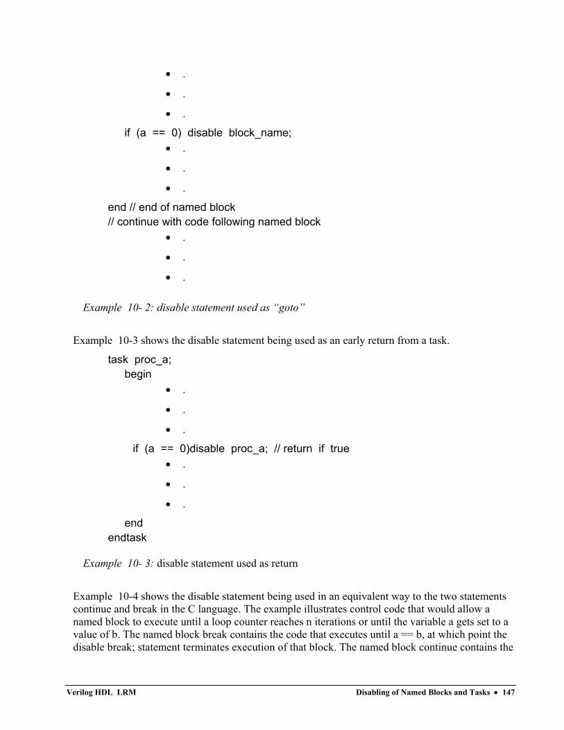
• .
• .
• .
if (a == 0) disable block_name; • .
• .
• .
end // end of named block // continue with code following named block
• .
• .
• .
Example 10- 2: disable statement used as “goto”
Example 10-3 shows the disable statement being used as an early return from a task.
task proc_a; begin
• .
• .
• .
if (a == 0)disable proc_a; // return if true • .
• .
• .
end endtask
Example 10- 3: disable statement used as return
Example 10-4 shows the disable statement being used in an equivalent way to the two statements continue and break in the C language. The example illustrates control code that would allow a named block to execute until a loop counter reaches n iterations or until the variable a gets set to a value of b. The named block break contains the code that executes until a == b, at which point the disable break; statement terminates execution of that block. The named block continue contains the
Verilog HDL LRM Disabling of Named Blocks and Tasks • 147
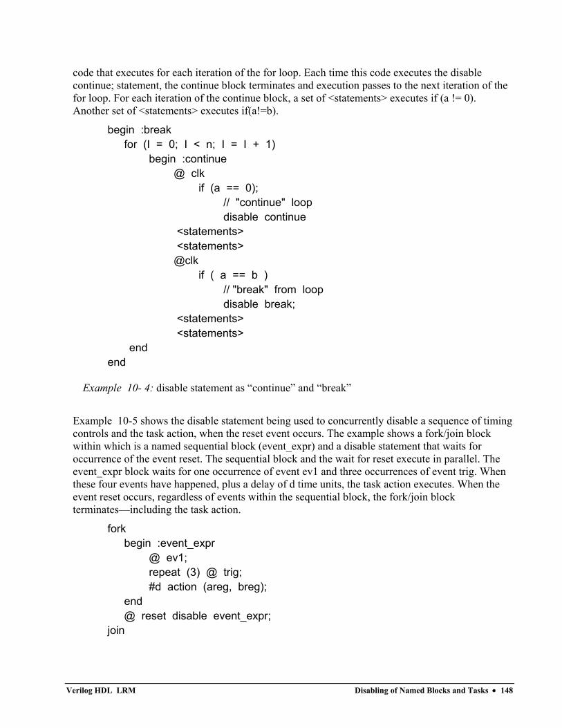
code that executes for each iteration of the for loop. Each time this code executes the disable continue; statement, the continue block terminates and execution passes to the next iteration of the for loop. For each iteration of the continue block, a set of <statements> executes if (a != 0). Another set of <statements> executes if(a!=b).
begin :break for (I = 0; I < n; I = I + 1) begin :continue @ clk if (a == 0); // "continue" loop disable continue <statements> <statements> @clk if ( a == b ) // "break" from loop disable break; <statements> <statements> end end
Example 10- 4: disable statement as “continue” and “break”
Example 10-5 shows the disable statement being used to concurrently disable a sequence of timing controls and the task action, when the reset event occurs. The example shows a fork/join block within which is a named sequential block (event_expr) and a disable statement that waits for occurrence of the event reset. The sequential block and the wait for reset execute in parallel. The event_expr block waits for one occurrence of event ev1 and three occurrences of event trig. When these four events have happened, plus a delay of d time units, the task action executes. When the event reset occurs, regardless of events within the sequential block, the fork/join block terminates—including the task action.
fork begin :event_expr @ ev1; repeat (3) @ trig; #d action (areg, breg); end @ reset disable event_expr; join
Verilog HDL LRM Disabling of Named Blocks and Tasks • 148
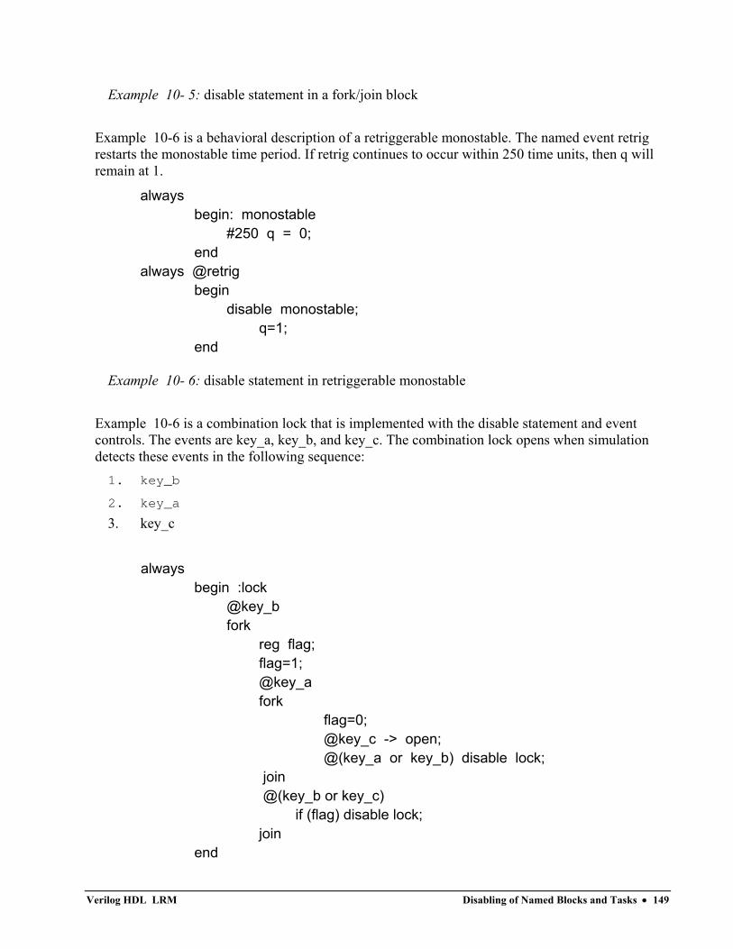
Example 10- 5: disable statement in a fork/join block
Example 10-6 is a behavioral description of a retriggerable monostable. The named event retrig restarts the monostable time period. If retrig continues to occur within 250 time units, then q will remain at 1.
always begin: monostable #250 q = 0; end always @retrig begin disable monostable; q=1; end
Example 10- 6: disable statement in retriggerable monostable
Example 10-6 is a combination lock that is implemented with the disable statement and event controls. The events are key_a, key_b, and key_c. The combination lock opens when simulation detects these events in the following sequence: 1. key_b
2. key_a
3. key_c
always begin :lock @key_b fork reg flag; flag=1; @key_a fork flag=0; @key_c -> open; @(key_a or key_b) disable lock; join @(key_b or key_c) if (flag) disable lock; join end
Verilog HDL LRM Disabling of Named Blocks and Tasks • 149
always @open begin disable lock; open_it_up; end
Example 10- 7: disable statement used with event controls
Verilog HDL LRM Disabling of Named Blocks and Tasks • 150
Procedural Continuous Assignments
11.0 Procedural Continuous Assignment Overview
The procedural continuous assignments are procedural statements that allow expressions to be driven continuously onto registers or nets. The syntax for these statements follows:
<statement> ::= assign <assignment> ;
<statement> ::= deassign <lvalue> ;
<force_statement> ::= force <assignment> ;
<release_statement> ::= release <lvalue> ;
Syntax 11- 1: Syntax for procedural continuous assignments
The left-hand side of the assignment in the assign statement is restricted to be a register reference or a concatenation of registers. It cannot be a memory element (array reference) or a bit-select or a part-select of a register.
In contrast, the left-hand side of the assignment in the force statement can be a register reference or a net reference, a bit-select or part-select of an expanded vector net. It can be a concatenation of any of the above. Bit-selects and part-selects of vector registers or unexpanded vector nets are not allowed, and will result in an error.
11.1 The assign and deassign Procedural Statements
The assign and deassign procedural statements allow continuous assignments to be placed onto registers for controlled periods of time. The assign procedural assignment statement overrides procedural assignments to a register. The deassign procedural statement ends a continuous assignment to a register. The assign and deassign procedural statements allow, for example, modeling of asynchronous clear/preset on a D-type edge-triggered flip-flop, where the clock is inhibited when the clear or preset is active.
Example 11-1 shows a use of the assign and deassign procedural statements in a behavioral description of a D-type flip-flop with preset and clear inputs.
Verilog HDL LRM Procedural Continuous Assignments • 151
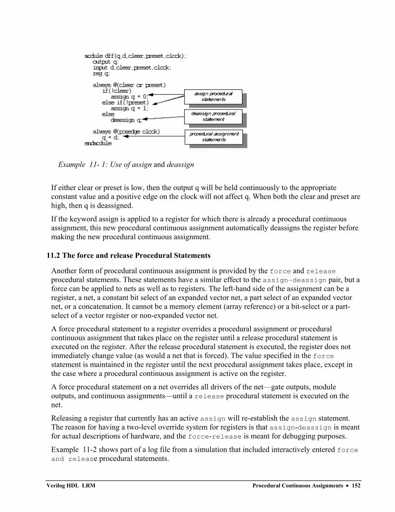
Example 11- 1: Use of assign and deassign
If either clear or preset is low, then the output q will be held continuously to the appropriate constant value and a positive edge on the clock will not affect q. When both the clear and preset are high, then q is deassigned.
If the keyword assign is applied to a register for which there is already a procedural continuous assignment, this new procedural continuous assignment automatically deassigns the register before making the new procedural continuous assignment.
11.2 The force and release Procedural Statements
Another form of procedural continuous assignment is provided by the force and release procedural statements. These statements have a similar effect to the assign-deassign pair, but a force can be applied to nets as well as to registers. The left-hand side of the assignment can be a register, a net, a constant bit select of an expanded vector net, a part select of an expanded vector net, or a concatenation. It cannot be a memory element (array reference) or a bit-select or a part-select of a vector register or non-expanded vector net.
A force procedural statement to a register overrides a procedural assignment or procedural continuous assignment that takes place on the register until a release procedural statement is executed on the register. After the release procedural statement is executed, the register does not immediately change value (as would a net that is forced). The value specified in the force statement is maintained in the register until the next procedural assignment takes place, except in the case where a procedural continuous assignment is active on the register.
A force procedural statement on a net overrides all drivers of the net—gate outputs, module outputs, and continuous assignments—until a release procedural statement is executed on the net.
Releasing a register that currently has an active assign will re-establish the assign statement. The reason for having a two-level override system for registers is that assign-deassign is meant for actual descriptions of hardware, and the force-release is meant for debugging purposes.
Example 11-2 shows part of a log file from a simulation that included interactively entered force and release procedural statements.
Verilog HDL LRM Procedural Continuous Assignments • 152
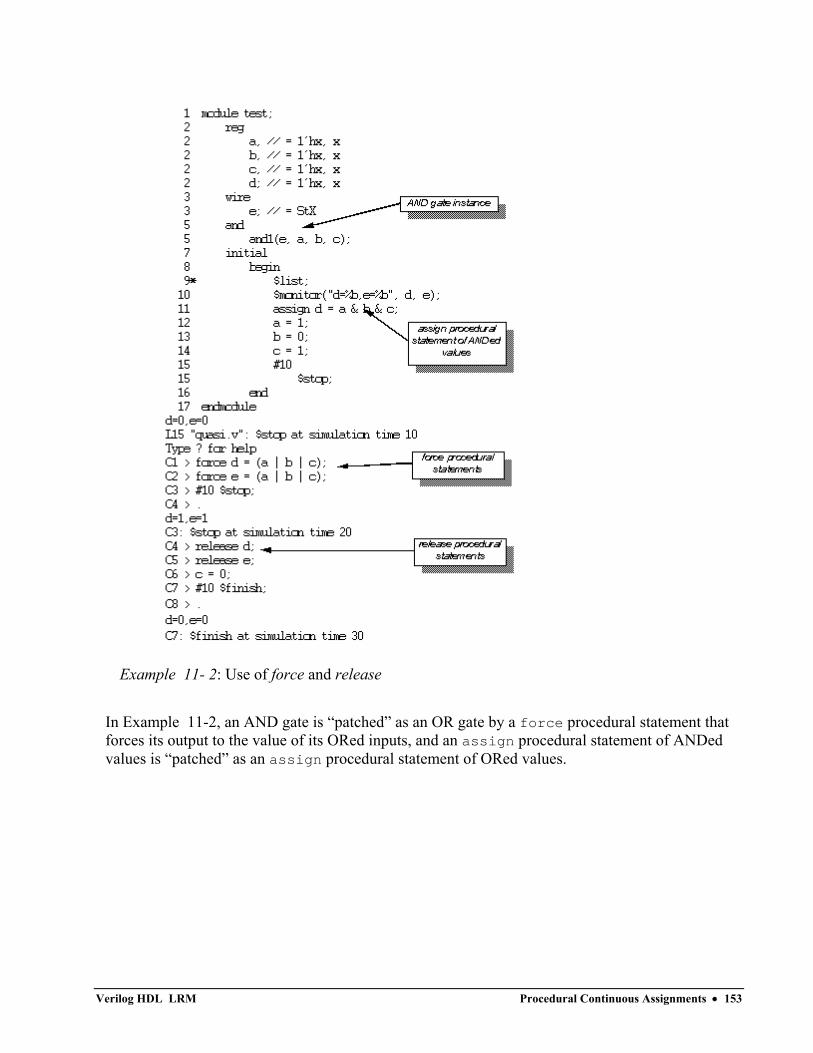
Example 11- 2: Use of force and release
In Example 11-2, an AND gate is “patched” as an OR gate by a force procedural statement that forces its output to the value of its ORed inputs, and an assign procedural statement of ANDed values is “patched” as an assign procedural statement of ORed values.
Verilog HDL LRM Procedural Continuous Assignments • 153
Hierarchical Structures
12.0 Hierarchical Structures Overview
The Verilog HDL supports a hierarchical hardware description structure by allowing modules to be embedded within other modules. Higher-level modules create instances of lower-level modules and communicate with them through input, output, and bidirectional ports. These module input/output ports can be scalar or vector.
As an example of a module hierarchy, consider a system consisting of printed circuit boards. The system would be represented as the top-level module and would create instances of modules that represent the boards. The board modules would, in turn, create instances of modules that represent ICs, and the ICs could, in turn, create instances of modules that represent predefined cells such as flip-flops, mux’s, and alu’s.
To describe a hierarchy of modules, the user provides textual definitions of the various modules. Each module definition stands alone; the definitions are not nested. Statements within the module definitions create instances of other modules, thus describing the hierarchy.
12.1 Modules
This section gives the formal syntax for a module definition and then gives the syntax for module instantiation, along with an example of a module definition and a module instantiation.
A module definition is enclosed between the keywords module and endmodule, where the <IDENTIFIER> after module gives the name of the module. The optional <list_of_ports> specifies an ordered list of the module’s IO ports. The order used can be significant when instantiating the module (see Section 12.1.2 Module Instantiation). The identifiers in this list must be declared in input, output, and inout statements within the module definition. The <module_items> define what constitutes a module, and include many different types of declarations and definitions; many of them have already been introduced.
<module> ::= module <name_of_module><list_of_ports>? ; <module_item>* endmodule
<name_of_module> ::=<IDENTIFIER>
<list_of_ports> ::=(<port><,<port>>*)
<module_item> ::=<parameter_declaration> ||=<input_declaration> ||=<output_declaration>
Verilog HDL LRM Hierarchical Structures • 154
||=<inout_declaration> ||=<net_declaration> ||=<reg_declaration> ||=<time_declaration> ||=<integer_declaration> ||=<real_declaration> ||=<event_declaration> ||=<gate_instantiation> ||=<primitive_instantiation> ||=<module_instantiation> ||=<parameter_override> ||=<continuous_assign> ||= <specify_block> ||=<initial_statement> ||=<always_statement> ||=<task> ||=<function>
Syntax 12- 1: Syntax definitions for <module>
See Section 12.4 Ports for the definitions of the syntax item <port>. See Section 12.1.3 Module Definition and Instance Example.
12.1.1 Top-Level Modules
Top-level modules are modules that are included in the source text supplied as input to a particular simulation run, but are not instantiated, as described in Section 12.1.2 Module Instantiation.
12.1.2 Module Instantiation
Instantiation allows one module to incorporate a copy of another module into itself. Module definitions do not nest. That is, one module definition cannot contain the text of another module definition within its module/endmodule keyword pair. A module definition nests another module by instantiating it. The <module_instantiation> statement creates one or more named instances of a defined module. For example, a counter module might instantiate a D flip-flop module to create eight instances of the flip-flop.
The following is the syntax for specifying instantiations of modules:
<module_instantiation> ::= <name_of_module> <parameter_value_assignment>? <module_instance>
<,<module_instance>>* ;
<name_of_module>
Verilog HDL LRM Hierarchical Structures • 155
::= <IDENTIFIER>
<parameter_value_assignment> ::= # ( <expression> <,<expression>>* )
<module_instance> ::= <name_of_instance> ( <list_of_module_connections>? )
<name_of_instance> ::= <IDENTIFIER>
<list_of_module_connections> ::= <module_port_connection> <,<module_port_connection>>* ||= <named_port_connection> <,<named_port_connection>>*
<module_port_connection> ::= <expression> ||= <NULL>
<named_port_connection> ::= .<IDENTIFIER> ( <expression> )
Syntax 12- 2: Definitions for <module_instantiation>
The definition for <named_port_connection> includes an <IDENTIFIER> token that can be satisfied only with a port name from the definition of the module being instantiated. See Section 12.4.4 Connecting Module Ports by Name for more details.
12.1.3 Module Definition and Instance Example
The code in Example 12-1 illustrates a circuit (the lower-level module) being driven by a simple waveform description (the higher-level module) where the circuit module is instantiated inside the waveform module.
// THE LOWER-LEVEL MODULE: //module description of an and flip-flop circuit module ffnand (q, qbar, preset, clear);
output q, qbar; //declares 2 circuit output nets input preset, clear; //declares 2 circuit input nets nand
// declaration of two nand gates and // their interconnections g1 (q, qbar, preset), g2 (qbar ,q, clear);
Verilog HDL LRM Hierarchical Structures • 156
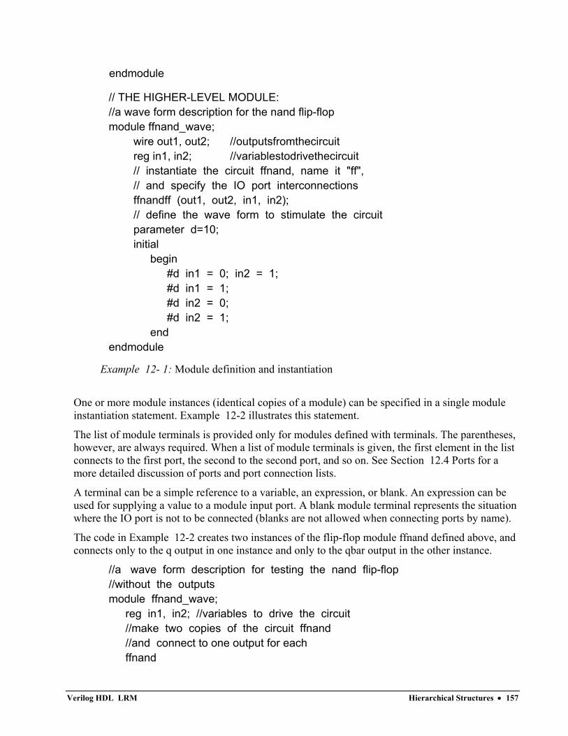
endmodule
// THE HIGHER-LEVEL MODULE: //a wave form description for the nand flip-flop module ffnand_wave;
wire out1, out2; //outputsfromthecircuit reg in1, in2; //variablestodrivethecircuit // instantiate the circuit ffnand, name it "ff", // and specify the IO port interconnections ffnandff (out1, out2, in1, in2); // define the wave form to stimulate the circuit parameter d=10; initial
begin #d in1 = 0; in2 = 1; #d in1 = 1; #d in2 = 0; #d in2 = 1;
end endmodule
Example 12- 1: Module definition and instantiation
One or more module instances (identical copies of a module) can be specified in a single module instantiation statement. Example 12-2 illustrates this statement.
The list of module terminals is provided only for modules defined with terminals. The parentheses, however, are always required. When a list of module terminals is given, the first element in the list connects to the first port, the second to the second port, and so on. See Section 12.4 Ports for a more detailed discussion of ports and port connection lists.
A terminal can be a simple reference to a variable, an expression, or blank. An expression can be used for supplying a value to a module input port. A blank module terminal represents the situation where the IO port is not to be connected (blanks are not allowed when connecting ports by name).
The code in Example 12-2 creates two instances of the flip-flop module ffnand defined above, and connects only to the q output in one instance and only to the qbar output in the other instance.
//a wave form description for testing the nand flip-flop //without the outputs module ffnand_wave; reg in1, in2; //variables to drive the circuit //make two copies of the circuit ffnand //and connect to one output for each ffnand
Verilog HDL LRM Hierarchical Structures • 157
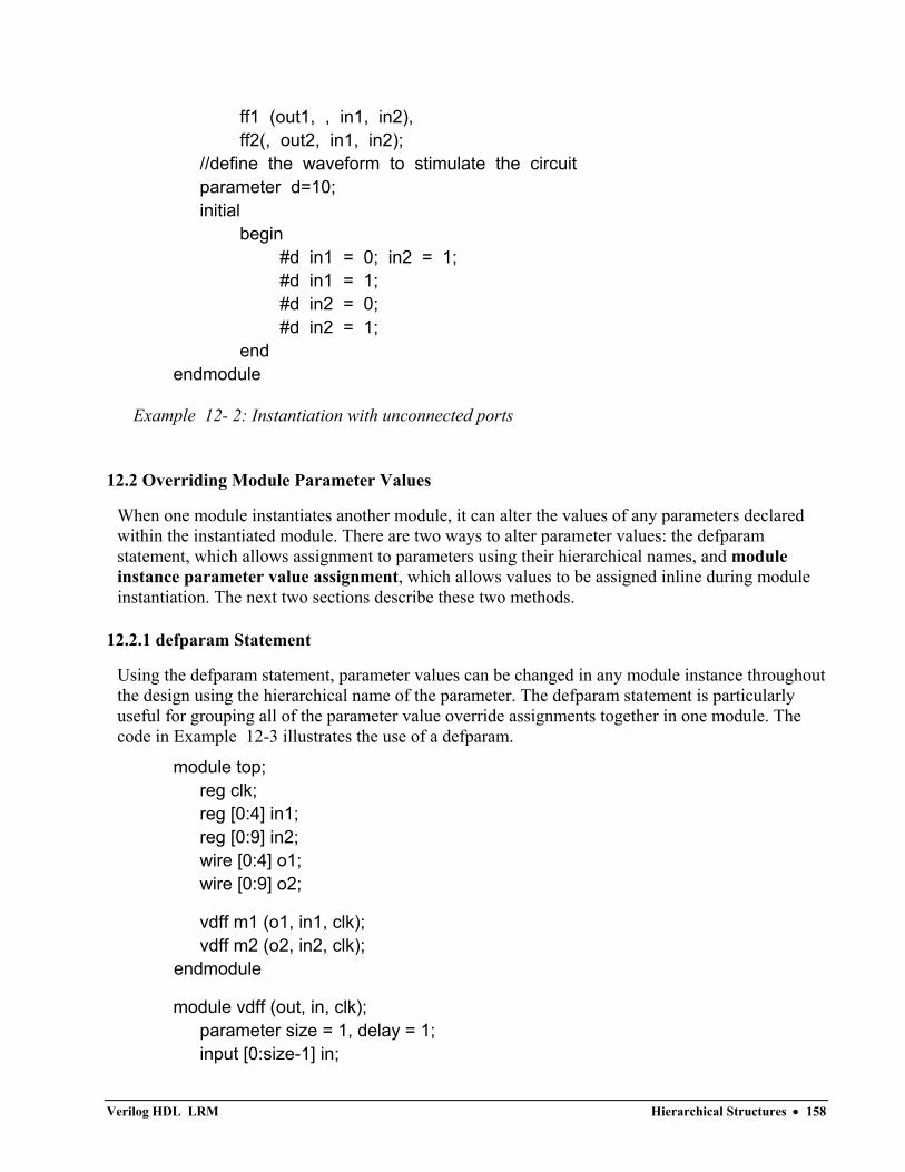
ff1 (out1, , in1, in2), ff2(, out2, in1, in2); //define the waveform to stimulate the circuit parameter d=10; initial begin #d in1 = 0; in2 = 1; #d in1 = 1; #d in2 = 0; #d in2 = 1; end endmodule
Example 12- 2: Instantiation with unconnected ports
12.2 Overriding Module Parameter Values
When one module instantiates another module, it can alter the values of any parameters declared within the instantiated module. There are two ways to alter parameter values: the defparam statement, which allows assignment to parameters using their hierarchical names, and module instance parameter value assignment, which allows values to be assigned inline during module instantiation. The next two sections describe these two methods.
12.2.1 defparam Statement
Using the defparam statement, parameter values can be changed in any module instance throughout the design using the hierarchical name of the parameter. The defparam statement is particularly useful for grouping all of the parameter value override assignments together in one module. The code in Example 12-3 illustrates the use of a defparam.
module top; reg clk; reg [0:4] in1; reg [0:9] in2; wire [0:4] o1; wire [0:9] o2;
vdff m1 (o1, in1, clk); vdff m2 (o2, in2, clk); endmodule
module vdff (out, in, clk); parameter size = 1, delay = 1; input [0:size-1] in;
Verilog HDL LRM Hierarchical Structures • 158
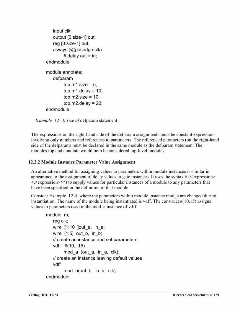
input clk; output [0:size-1] out; reg [0:size-1] out; always @(posedge clk) # delay out = in; endmodule
module annotate; defparam top.m1.size = 5, top.m1.delay = 10, top.m2.size = 10, top.m2.delay = 20; endmodule
Example 12- 3: Use of defparam statement
The expressions on the right-hand side of the defparam assignments must be constant expressions involving only numbers and references to parameters. The referenced parameters (on the right-hand side of the defparam) must be declared in the same module as the defparam statement. The modules top and annotate would both be considered top-level modules.
12.2.2 Module Instance Parameter Value Assignment
An alternative method for assigning values to parameters within module instances is similar in appearance to the assignment of delay values to gate instances. It uses the syntax # (<expression> <,<expression>>*) to supply values for particular instances of a module to any parameters that have been specified in the definition of that module.
Consider Example 12-4, where the parameters within module instance mod_a are changed during instantiation. The name of the module being instantiated is vdff. The construct #(10,15) assigns values to parameters used in the mod_a instance of vdff.
module m; reg clk; wire [1:10 ]out_a, in_a; wire [1:5] out_b, in_b; // create an instance and set parameters vdff #(10, 15) mod_a (out_a, in_a, clk); // create an instance leaving default values vdff mod_b(out_b, in_b, clk); endmodule
Verilog HDL LRM Hierarchical Structures • 159
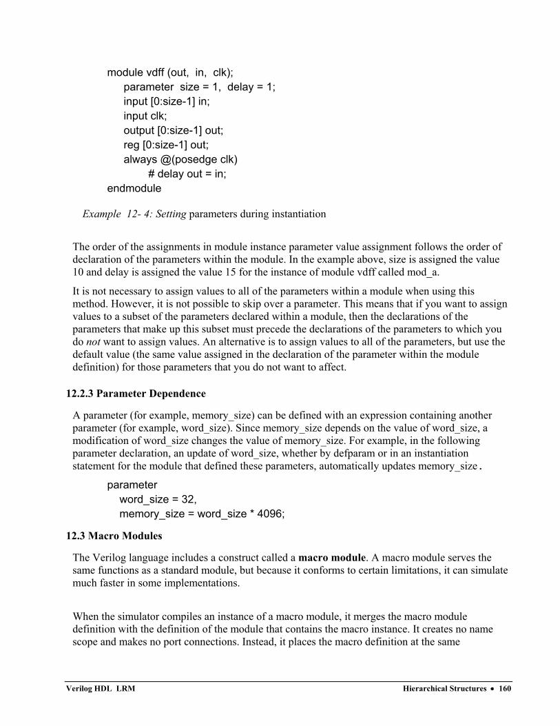
module vdff (out, in, clk); parameter size = 1, delay = 1; input [0:size-1] in; input clk; output [0:size-1] out; reg [0:size-1] out; always @(posedge clk) # delay out = in; endmodule
Example 12- 4: Setting parameters during instantiation
The order of the assignments in module instance parameter value assignment follows the order of declaration of the parameters within the module. In the example above, size is assigned the value 10 and delay is assigned the value 15 for the instance of module vdff called mod_a.
It is not necessary to assign values to all of the parameters within a module when using this method. However, it is not possible to skip over a parameter. This means that if you want to assign values to a subset of the parameters declared within a module, then the declarations of the parameters that make up this subset must precede the declarations of the parameters to which you do not want to assign values. An alternative is to assign values to all of the parameters, but use the default value (the same value assigned in the declaration of the parameter within the module definition) for those parameters that you do not want to affect.
12.2.3 Parameter Dependence
A parameter (for example, memory_size) can be defined with an expression containing another parameter (for example, word_size). Since memory_size depends on the value of word_size, a modification of word_size changes the value of memory_size. For example, in the following parameter declaration, an update of word_size, whether by defparam or in an instantiation statement for the module that defined these parameters, automatically updates memory_size.
parameter word_size = 32, memory_size = word_size * 4096;
12.3 Macro Modules
The Verilog language includes a construct called a macro module. A macro module serves the same functions as a standard module, but because it conforms to certain limitations, it can simulate much faster in some implementations.
When the simulator compiles an instance of a macro module, it merges the macro module definition with the definition of the module that contains the macro instance. It creates no name scope and makes no port connections. Instead, it places the macro definition at the same
Verilog HDL LRM Hierarchical Structures • 160
hierarchical level as the containing module. This process is called macro module expansion. A compiled macro module instance is said to be expanded.
12.3.1 Specifying Macro Modules
Macro modules are specified by using the keyword macromodule in place of the keyword module in the module definition. Example 12-5 defines a macro module called NAND2.
macromodule NAND2 (q, a, b); output q; input a, b; nand (q,a,b); endmodule
Example 12- 5: Defining a macro module
12.3.2 Instances of Macro Modules
Instances of macro modules are specified in exactly the same way as instances of normal modules.
12.4 Ports
Ports provide a means of interconnecting a hardware description consisting of modules, primitives, and macro modules. For example, module A can instantiate module B, using port connections appropriate to module A. These port names can differ from the names of the internal nets and registers specified in the definition of module B, but the connection is still made.
12.4.1 Port Definition
The syntax for a port is given below (this is the completion of the syntax presented in Section 12.1 Modules).
<port> : :=<port_expression>? ||=.<name_of_port>( <port_expression>? )
<port_expression> ::=<port_reference> ||={ <port_reference> <,<port_reference>>* }
<port_reference> ::= <name_of_variable> ||= <name_of_variable> [ <constant_expression> ] ||= <name_of_variable> [ <constant_expression> : <constant_expression> ]
Verilog HDL LRM Hierarchical Structures • 161
<name_of_port> ::= <IDENTIFIER>
Syntax 12- 3: Definitions for <port>
The <port_expression> syntax item in the <port> definition can be one of the following:
• a simple identifier
• a bit-select of a vector declared within the module
• a part-select of a vector declared within the module
• a concatenation of any of the above
Note that the <port_expression> is optional because ports can be defined that do not connect to anything internal to the module.
Note also that the two types of module port connections cannot be mixed; connections to the ports of a particular module instance must be all by position or all by name.
12.4.2 Port Declarations
Each port listed in the module definition’s <list_of_ports> must be declared in the body of the module as an input, output, or bidirectional inout. This is in addition to any other declaration for a particular port— for example, a net, reg, or wire. The syntax for port declarations is as follows:
<input_declaration> ::=input<range>?<list_of_variables>;
<output_declaration> ::=output<range>?<list_of_variables>;
<inout_declaration> ::=inout<range>?<list_of_variables>;
Syntax 12- 4: Definitions for <port_declarations>
12.4.3 Connecting Module Ports by Ordered List
One method of making the connection between the ports listed in a module instantiation and the ports defined by the instantiated module is the ordered list—that is, the ports listed for the module instance are in the same order as the ports listed in the module definition.
Example 12-6 illustrates a top-level module (topmod) that instantiates a second module (modB). Module modB has ports that are connected by an ordered list. The connections made are as follows:
Verilog HDL LRM Hierarchical Structures • 162
• Port wa in the modB definition connects to the bit-select v[0] in the topmod module.
• Port wb connects to v[3].
• Port c connects to w.
• Port d connects to v[4].
In the modB definition, ports wa and wb are declared as inouts while ports c and d are declared as input.
module topmod; wire [4:0] v; wire a, b, c, w;
• .
• .
• .
modB b1 (v[0], v[3], w, v[4]); • .
• .
• .
endmodule module modB (wa, wb, c, d); inout wa, wb; input c, d; tranif1 g1(wa, wb, cinvert); not #(2, 6) (cinvert, int); and #(6, 5) g2 (int, c, d); endmodule
Example 12- 6: Port connections using ordered list
During simulation of the b1 instance of modb, the and gate activates first to produce a value on int. This value triggers the not gate to produce output on cinvert, which then activates the tranif1 gate g1.
12.4.4 Connecting Module Ports by Name
The second way to connect module ports consists of explicitly linking the two names for each side of the connection—the name used in the module definition, followed by the name used in the instantiating module. This compound name is then placed in the list of module connections. The following is the syntax for connection by name:
Verilog HDL LRM Hierarchical Structures • 163
.<name_of_port>(<port_expression>?)
The <name_of_port> is the name specified in the module definition. The <name_of_port> cannot be a bit select, part select, or a concatenation of ports.
The <port_expression> is the name used by the instantiating module and can be one of the following:
• a simple identifier
• a bit-select of a vector declared within the module
• a part-select of a vector declared within the module
• a concatenation of any of the above
The <port_expression> is optional so that the instantiating module can document the existence of the port without connecting it to anything. The parentheses are not optional.
In the following example, the instantiating module connects its signals topA and topB to the ports In1 and Out defined by the module ALPHA. At least one port provided by ALPHA is unused; it is named In2. There could be other unused ports not mentioned in the instantiation.
ALPHA instance1 (.Out(topB),.In1(topA),.In2());
Example 12-7 defines the modules modB and topmod and then topmod instantiates modB using ports connected by name.
module topmod; wire [4:0] v; wire a, b, c, w; modB b1 (.wb(v[3]), .wa(v[0]), .d(v[4]), .c(w)); endmodule
module modB (wa, wb, c, d); inout wa, wb; input c, d; tranif1 g1(wa, wb, cinvert); not #(6, 2) (cinvert, int); and #(5, 6) g2(int, c, d) endmodule
Example 12- 7: Connecting ports by name
Note that because these connections are made by name, the order in which they appear is irrelevant.
Verilog HDL LRM Hierarchical Structures • 164
12.4.5 Real Numbers in Port Connections
The real data type cannot be directly connected to a port, but rather must be connected indirectly, as shown in Example 12-8. The system functions $realtobits and $bitstoreal are used for passing the bit patterns across module ports. (See Appendix B, B.8 Functions and Tasks for Reals, for a description of these system tasks.)
module driver (net_r); output net_r; real r; wire [64:1] net_r = $realtobits(r); endmodule module receiver (net_r); input net_r; wire [64:1] net_r; real r; initial assign r = $bitstoreal(net_r); endmodule
Example 12- 8: Connecting reals to a port
12.4.6 Port Collapsing
A port of a module can be viewed as providing a link or connection between two items (nets, registers, expressions, and so on)—one internal to the module instance and one external to the module instance. Wherever it is possible, the some tools collapse port connections during processing—that is, the two items become one entity. Both names continue to exist for reference purposes, but, internally, the simulator eliminates one of the items. This corresponds to the physical case where a net described at two levels of a Verilog HDL hierarchy is actually just one wire.
Examination of the port connection rules described below will show that the item receiving the value of the port (the inside item for inputs, the outside item for outputs) must be a net. The item which provides the value can be any expression, but port collapsing is only possible if both items are nets. Expressions such as (a+b) as the outside item in a module port connection preclude collapsing of that port.
12.4.7 Port Connection Rules
The following rules govern the way module ports are declared and the way they are interconnected:
Rule 1:
An input or inout port must be declared as a net type.
Rule 2:
Verilog HDL LRM Hierarchical Structures • 165
Each port connection is a continuous “assignment” of source to sink, where one connected item is a signal source and the other is a signal sink. Only nets are permitted to be the sinks in an assignment.
Both scalar and vector nets are permitted. The output and input ports of a module are by definition connected to signal source items internal to the module. The following external items cannot be connected to the output or input ports of modules:
• registers
• expressions other than:
• a scalar net
• a vector net
• a constant bit select of a vector net
• a part select of a vector net
• a concatenation of the expressions listed above
In port collapsing, the two items that are connected through a module port—one being external to the module, the other being internal to the module—are merged into a single item. Not every port can be collapsed. The following rule defines when port collapsing occurs:
Rule 3:
A module port is collapsed only if:
• the port connects two nets, and
• the connected nets are either both scalars or have the same vector size.
Vector nets are split into scalar bits in order to increase the amount of port collapsing that occurs in a circuit. Splitting causes a vector net to be internally represented as a collection of scalars, thus allowing Rule 3 to be applied. This occurs whenever the items on both sides of the port are nets, and at least one of them is a bit select or part select of a vector net or the net is specified with the keyword scalared.
Given Rule 3, it is clear that only ports that connect nets can be collapsed. But what happens if the nets on either side of the port are of different net types—for example, one is a triand and the other is a tri? When different net types are connected through a module port and the port can be collapsed, the resulting net type is determined based on Rule 4. In Rule 4, the term “dominating net type” is used in the following sense: A net type A “dominates” a net type B if, with identical signal sources on the two net types, either (a) the state on B is the same as that on A or (b) the state on B is not completely known but does not conflict with the state on A (for example, X does not conflict with 1 or 0; H does not conflict with Z or 1; and so on).
Rule 4:
When the two nets connected by a collapsed port are of different net type, the resulting single net is assigned one of the following:
Verilog HDL LRM Hierarchical Structures • 166
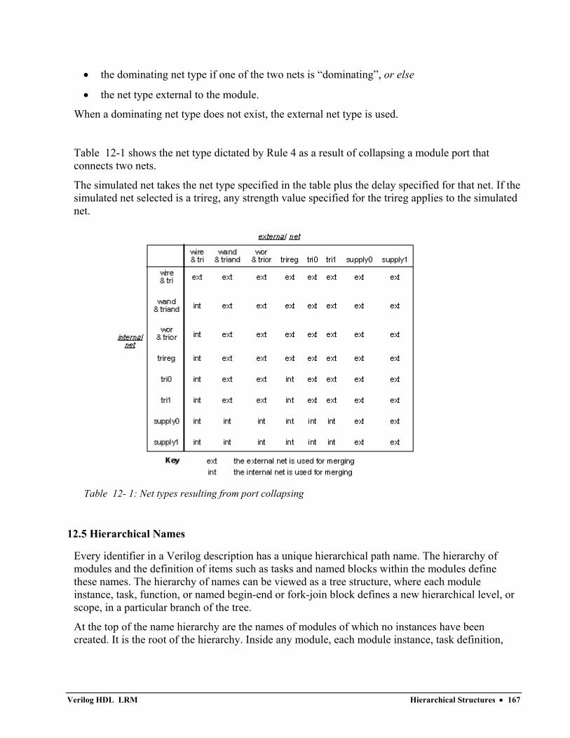
• the dominating net type if one of the two nets is “dominating”, or else
• the net type external to the module.
When a dominating net type does not exist, the external net type is used.
Table 12-1 shows the net type dictated by Rule 4 as a result of collapsing a module port that connects two nets.
The simulated net takes the net type specified in the table plus the delay specified for that net. If the simulated net selected is a trireg, any strength value specified for the trireg applies to the simulated net.
Table 12- 1: Net types resulting from port collapsing
12.5 Hierarchical Names
Every identifier in a Verilog description has a unique hierarchical path name. The hierarchy of modules and the definition of items such as tasks and named blocks within the modules define these names. The hierarchy of names can be viewed as a tree structure, where each module instance, task, function, or named begin-end or fork-join block defines a new hierarchical level, or scope, in a particular branch of the tree.
At the top of the name hierarchy are the names of modules of which no instances have been created. It is the root of the hierarchy. Inside any module, each module instance, task definition,
Verilog HDL LRM Hierarchical Structures • 167
function definition, and named begin-end or fork-join block defines a new branch of the hierarchy. Named blocks within named blocks and within tasks and functions also create new branches.
Each node in the hierarchical name tree is a separate scope with respect to identifiers. A particular identifier can be declared at most once in any scope. See Section 12.6 Scope Rules, for a discussion of scope rules.
Any named Verilog object can be referenced uniquely in its full form by concatenating the names of the modules, tasks, functions, or blocks that contain it. Use the period character to separate each of the names in the hierarchy. The complete path name to any object starts at a top-level module. This path name can be used from any level in the description. The first node name in this path name can also be the top of a hierarchy that starts at the level where the path is being used.
The code in Example 12-9 defines a hierarchy of module instances and named blocks. Figure 12-1 illustrates the hierarchy implicit in this Verilog code. Figure 12-2 is a list of the hierarchical forms of the names of all the objects defined in the code.
module mod ( in ); input in; always @ ( posedge in )
begin :keep reg hold; hold = in; end
endmodule
module cct (stim1, stim2); input stim1, stim2; // instantiate mod modamod (stim1), bmod (stim2);
endmodule
module wave; reg stim1, stim2; // instantiate cct ccta (stim1, stim2); initial
begin :wave1 #100 fork :innerwave
reg hold; join #150 begin
stim1=0;
Verilog HDL LRM Hierarchical Structures • 168
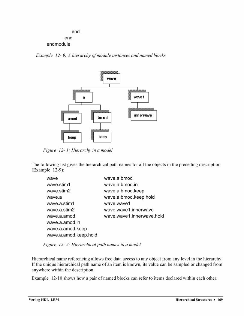
end end
endmodule
Example 12- 9: A hierarchy of module instances and named blocks
Figure 12- 1: Hierarchy in a model
The following list gives the hierarchical path names for all the objects in the preceding description (Example 12-9):
wave wave.a.bmod wave.stim1 wave.a.bmod.in wave.stim2 wave.a.bmod.keep wave.a wave.a.bmod.keep.hold wave.a.stim1 wave.wave1 wave.a.stim2 wave.wave1.innerwave wave.a.amod wave.wave1.innerwave.hold wave.a.amod.in wave.a.amod.keep wave.a.amod.keep.hold
Figure 12- 2: Hierarchical path names in a model
Hierarchical name referencing allows free data access to any object from any level in the hierarchy. If the unique hierarchical path name of an item is known, its value can be sampled or changed from anywhere within the description.
Example 12-10 shows how a pair of named blocks can refer to items declared within each other.
Verilog HDL LRM Hierarchical Structures • 169
begin fork :mod_1 reg x; mod_2.x = 1;
• .
• .
• .
join fork :mod_2 reg x; mod_1.x = 0;
• .
• .
• .
join end
Example 12- 10: Using hierarchical names across blocks
12.5.1 Upwards Name Referencing
The name of a module is sufficient to identify the module and its location in the hierarchy. A lower-level module can reference items in a module above it in the hierarchy if the name of the higher-level module is known. The syntax for an upward reference is as follows: <name_of_module>.<name_of_item>
There can be no spaces within the reference. Example 12-11 demonstrates upward referencing. In this example, there are four modules, mod_a, mod_b, mod_c, and mod_d. Each module contains an integer x. The highest-level modules in this segment of a model hierarchy are mod_a and mod_d. There are two copies of module mod_b.x because both mod_a and mod_d both instantiate mod_b.x. There are four copies of mod_c.x because each of the two copies of mod_b.x instantiates mod_c.x twice.
module mod_a; integer x; mod_b inst_b1(); endmodule module mod_b; integer x; mod_c inst_c1(), inst_c2();
Verilog HDL LRM Hierarchical Structures • 170
initial #10 inst_c1.x = 2; //downward path - //references 2 copies of x: //mod_a.inst_b1.inst_c1.x //mod_d.inst_b1.inst_c1.x
endmodule
module mod_c; integer x; initial begin x = 1; //local name references //4 copies of x: //mod_a.inst_b1.inst_c1.x //mod_a.inst_b1.inst_c2.x //mod_d.inst_b1.inst_c1.x //mod_d.inst_b1.inst_c2.x mod_b.x = 1; //upward path references 2 //copies of x: //mod_a.inst_b1..x //mod_a.inst_b1.inst_c2.x end
endmodule
module mod_d; integer x; mod_b inst_b1(); initial begin mod_a.x = 1; // full path name references each // copy of x mod_a.inst_b1.x = 2; mod_a.inst_b1.inst_c1.x = 3; mod_a.inst_b1.inst_c2.x = 4; mod_d.x = 5; mod_d.inst_b1.x = 6; mod_d.inst_b1.inst_c1.x = 7; mod_d.inst_b1.inst_c2.x = 8; end
endmodule
Example 12- 11: Upwards name referencing
Verilog HDL LRM Hierarchical Structures • 171
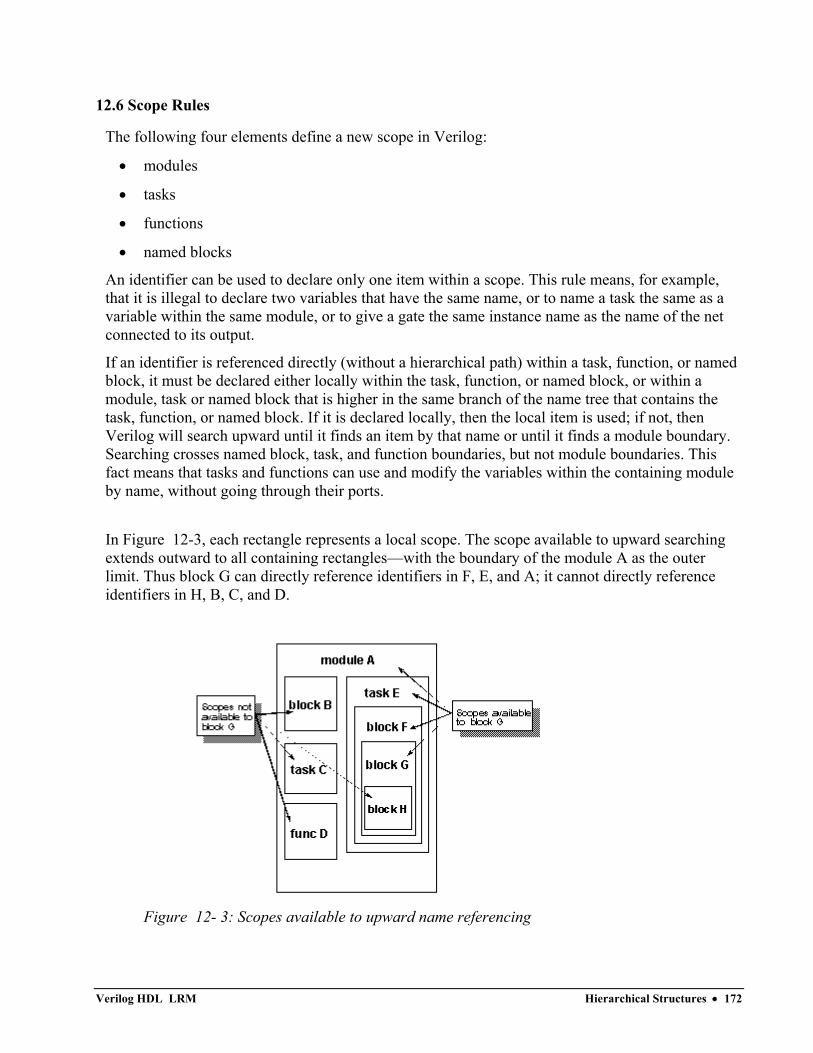
12.6 Scope Rules
The following four elements define a new scope in Verilog:
• modules
• tasks
• functions
• named blocks
An identifier can be used to declare only one item within a scope. This rule means, for example, that it is illegal to declare two variables that have the same name, or to name a task the same as a variable within the same module, or to give a gate the same instance name as the name of the net connected to its output.
If an identifier is referenced directly (without a hierarchical path) within a task, function, or named block, it must be declared either locally within the task, function, or named block, or within a module, task or named block that is higher in the same branch of the name tree that contains the task, function, or named block. If it is declared locally, then the local item is used; if not, then Verilog will search upward until it finds an item by that name or until it finds a module boundary. Searching crosses named block, task, and function boundaries, but not module boundaries. This fact means that tasks and functions can use and modify the variables within the containing module by name, without going through their ports.
In Figure 12-3, each rectangle represents a local scope. The scope available to upward searching extends outward to all containing rectangles—with the boundary of the module A as the outer limit. Thus block G can directly reference identifiers in F, E, and A; it cannot directly reference identifiers in H, B, C, and D.
Figure 12- 3: Scopes available to upward name referencing
Verilog HDL LRM Hierarchical Structures • 172
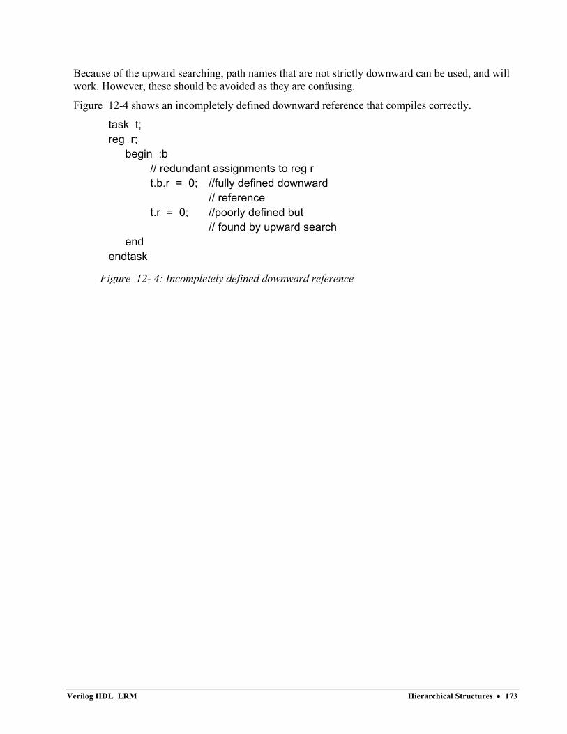
Because of the upward searching, path names that are not strictly downward can be used, and will work. However, these should be avoided as they are confusing.
Figure 12-4 shows an incompletely defined downward reference that compiles correctly.
task t; reg r; begin :b // redundant assignments to reg r t.b.r = 0; //fully defined downward // reference t.r = 0; //poorly defined but // found by upward search end endtask
Figure 12- 4: Incompletely defined downward reference
Verilog HDL LRM Hierarchical Structures • 173
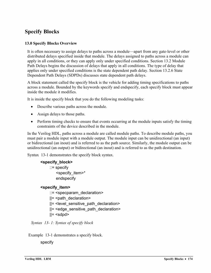
Specify Blocks
13.0 Specify Blocks Overview
It is often necessary to assign delays to paths across a module—apart from any gate-level or other distributed delays specified inside that module. The delays assigned to paths across a module can apply in all conditions, or they can apply only under specified conditions. Section 13.2 Module Path Delays begins the discussion of delays that apply in all conditions. The type of delay that applies only under specified conditions is the state dependent path delay. Section 13.2.6 State Dependent Path Delays (SDPDs) discusses state dependent path delays.
A block statement called the specify block is the vehicle for adding timing specifications to paths across a module. Bounded by the keywords specify and endspecify, each specify block must appear inside the module it modifies.
It is inside the specify block that you do the following modeling tasks:
• Describe various paths across the module.
• Assign delays to those paths.
• Perform timing checks to ensure that events occurring at the module inputs satisfy the timing constraints of the device described in the module.
In the Verilog HDL, paths across a module are called module paths. To describe module paths, you must pair a module input with a module output. The module input can be unidirectional (an input) or bidirectional (an inout) and is referred to as the path source. Similarly, the module output can be unidirectional (an output) or bidirectional (an inout) and is referred to as the path destination.
Syntax 13-1 demonstrates the specify block syntax.
<specify_block> ::= specify <specify_item>* endspecify
<specify_item> ::= <specparam_declaration> ||= <path_declaration> ||= <level_sensitive_path_declaration> ||= <edge_sensitive_path_declaration> ||= <sdpd>
Syntax 13- 1: Syntax of specify block
Example 13-1 demonstrates a specify block.
specify
Verilog HDL LRM Specify Blocks • 174
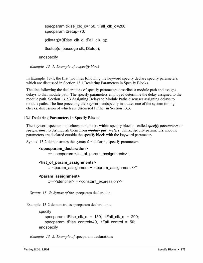
specparam tRise_clk_q=150, tFall_clk_q=200; specparam tSetup=70;
(clk=>q)=(tRise_clk_q, tFall_clk_q);
$setup(d, posedge clk, tSetup);
endspecify
Example 13- 1: Example of a specify block
In Example 13-1, the first two lines following the keyword specify declare specify parameters, which are discussed in Section 13.1 Declaring Parameters in Specify Blocks.
The line following the declarations of specify parameters describes a module path and assigns delays to that module path. The specify parameters employed determine the delay assigned to the module path. Section 13.2.3 Assigning Delays to Module Paths discusses assigning delays to module paths. The line preceding the keyword endspecify institutes one of the system timing checks, discussion of which are discussed further in Section 13.3.
13.1 Declaring Parameters in Specify Blocks
The keyword specparam declares parameters within specify blocks—called specify parameters or specparams, to distinguish them from module parameters. Unlike specify parameters, module parameters are declared outside the specify block with the keyword parameter.
Syntax 13-2 demonstrates the syntax for declaring specify parameters.
<specparam_declaration> ::= specparam <list_of_param_assignments> ;
<list_of_param_assignments> ::=<param_assignment><,<param_assignment>>*
<param_assignment> ::=<<identifier> = <constant_expression>>
Syntax 13- 2: Syntax of the specparam declaration
Example 13-2 demonstrates specparam declarations.
specify specparam tRise_clk_q = 150, tFall_clk_q = 200; specparam tRise_control=40, tFall_control = 50; endspecify
Example 13- 2: Example of specparam declarations
Verilog HDL LRM Specify Blocks • 175
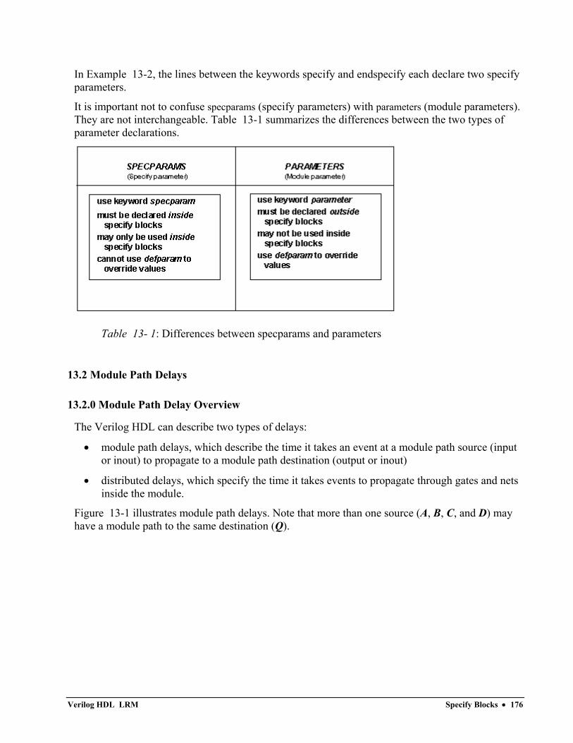
In Example 13-2, the lines between the keywords specify and endspecify each declare two specify parameters.
It is important not to confuse specparams (specify parameters) with parameters (module parameters). They are not interchangeable. Table 13-1 summarizes the differences between the two types of parameter declarations.
Table 13- 1: Differences between specparams and parameters
13.2 Module Path Delays
13.2.0 Module Path Delay Overview
The Verilog HDL can describe two types of delays:
• module path delays, which describe the time it takes an event at a module path source (input or inout) to propagate to a module path destination (output or inout)
• distributed delays, which specify the time it takes events to propagate through gates and nets inside the module.
Figure 13-1 illustrates module path delays. Note that more than one source (A, B, C, and D) may have a module path to the same destination (Q).
Verilog HDL LRM Specify Blocks • 176
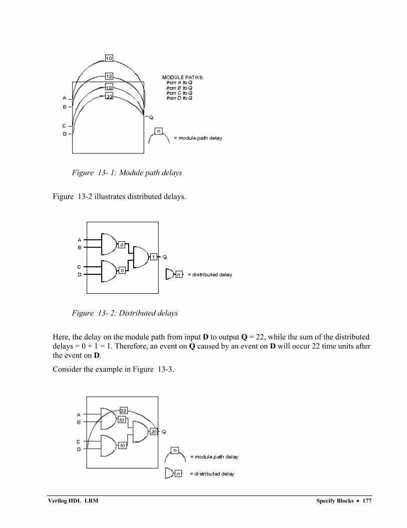
Figure 13- 1: Module path delays
Figure 13-2 illustrates distributed delays.
Figure 13- 2: Distributed delays
Here, the delay on the module path from input D to output Q = 22, while the sum of the distributed delays = 0 + 1 = 1. Therefore, an event on Q caused by an event on D will occur 22 time units after the event on D.
Consider the example in Figure 13-3.
Verilog HDL LRM Specify Blocks • 177
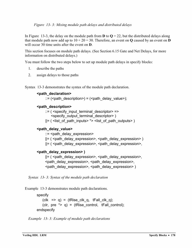
Figure 13- 3: Mixing module path delays and distributed delays
In Figure 13-3, the delay on the module path from D to Q = 22, but the distributed delays along that module path now add up to 10 + 20 = 30. Therefore, an event on Q caused by an event on D will occur 30 time units after the event on D.
This section focuses on module path delays. (See Section 6.15 Gate and Net Delays, for more information on distributed delays.)
You must follow the two steps below to set up module path delays in specify blocks:
1. describe the paths
2. assign delays to those paths
Syntax 13-3 demonstrates the syntax of the module path declaration.
<path_declaration> ::= (<path_description>) = (<path_delay_value>);
<path_description> ::= ( <specify_input_terminal_descriptor> =>
<specify_output_terminal_descriptor> ) ||= ( <list_of_path_inputs> *> <list_of_path_outputs> )
<path_delay_value> ::= <path_delay_expression> ||= ( <path_delay_expression>, <path_delay_expression> ) ||= ( <path_delay_expression>, <path_delay_expression>,
<path_delay_expression> ) ||= ( <path_delay_expression>, <path_delay_expression>, <path_delay_expression>, <path_delay_expression>, <path_delay_expression>, <path_delay_expression> )
Syntax 13- 3: Syntax of the module path declaration
Example 13-3 demonstrates module path declarations.
specify (clk => q) = (tRise_clk_q, tFall_clk_q); (clr, pre *> q) = (tRise_control, tFall_control); endspecify
Example 13- 3: Example of module path declarations
Verilog HDL LRM Specify Blocks • 178
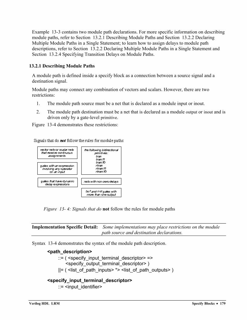
Example 13-3 contains two module path declarations. For more specific information on describing module paths, refer to Section 13.2.1 Describing Module Paths and Section 13.2.2 Declaring Multiple Module Paths in a Single Statement; to learn how to assign delays to module path descriptions, refer to Section 13.2.2 Declaring Multiple Module Paths in a Single Statement and Section 13.2.4 Specifying Transition Delays on Module Paths.
13.2.1 Describing Module Paths
A module path is defined inside a specify block as a connection between a source signal and a destination signal.
Module paths may connect any combination of vectors and scalars. However, there are two restrictions:
1. The module path source must be a net that is declared as a module input or inout.
2. The module path destination must be a net that is declared as a module output or inout and is driven only by a gate-level primitive.
Figure 13-4 demonstrates these restrictions:
Figure 13- 4: Signals that do not follow the rules for module paths
Implementation Specific Detail: Some implementations may place restrictions on the module path source and destination declarations.
Syntax 13-4 demonstrates the syntax of the module path description.
<path_description> ::= ( <specify_input_terminal_descriptor> =>
<specify_output_terminal_descriptor> ) ||= ( <list_of_path_inputs> *> <list_of_path_outputs> )
<specify_input_terminal_descriptor> ::= <input_identifier>
Verilog HDL LRM Specify Blocks • 179
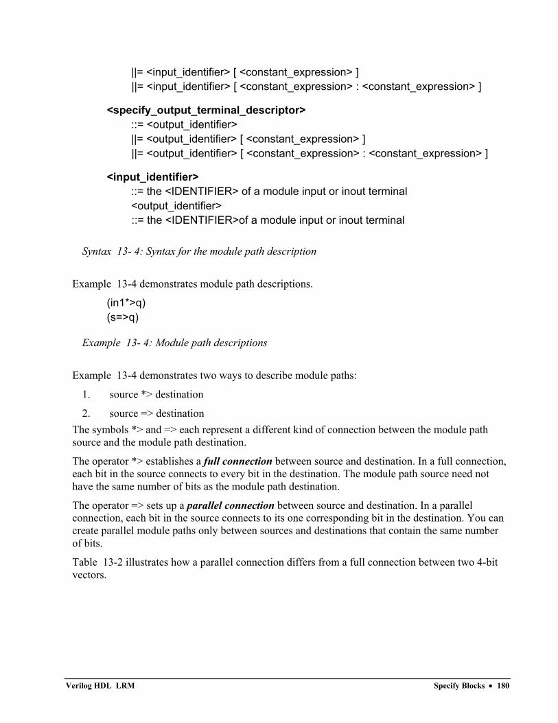
||= <input_identifier> [ <constant_expression> ] ||= <input_identifier> [ <constant_expression> : <constant_expression> ]
<specify_output_terminal_descriptor> ::= <output_identifier> ||= <output_identifier> [ <constant_expression> ] ||= <output_identifier> [ <constant_expression> : <constant_expression> ]
<input_identifier> ::= the <IDENTIFIER> of a module input or inout terminal <output_identifier> ::= the <IDENTIFIER>of a module input or inout terminal
Syntax 13- 4: Syntax for the module path description
Example 13-4 demonstrates module path descriptions.
(in1*>q) (s=>q)
Example 13- 4: Module path descriptions
Example 13-4 demonstrates two ways to describe module paths:
1. source *> destination
2. source => destination The symbols *> and => each represent a different kind of connection between the module path source and the module path destination.
The operator *> establishes a full connection between source and destination. In a full connection, each bit in the source connects to every bit in the destination. The module path source need not have the same number of bits as the module path destination.
The operator => sets up a parallel connection between source and destination. In a parallel connection, each bit in the source connects to its one corresponding bit in the destination. You can create parallel module paths only between sources and destinations that contain the same number of bits.
Table 13-2 illustrates how a parallel connection differs from a full connection between two 4-bit vectors.
Verilog HDL LRM Specify Blocks • 180
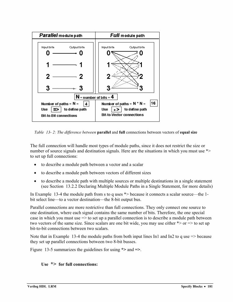
Table 13- 2: The difference between parallel and full connections between vectors of equal size
The full connection will handle most types of module paths, since it does not restrict the size or number of source signals and destination signals. Here are the situations in which you must use *> to set up full connections:
• to describe a module path between a vector and a scalar
• to describe a module path between vectors of different sizes
• to describe a module path with multiple sources or multiple destinations in a single statement (see Section 13.2.2 Declaring Multiple Module Paths in a Single Statement, for more details)
In Example 13-4 the module path from s to q uses *> because it connects a scalar source—the 1-bit select line—to a vector destination—the 8-bit output bus.
Parallel connections are more restrictive than full connections. They only connect one source to one destination, where each signal contains the same number of bits. Therefore, the one special case in which you must use => to set up a parallel connection is to describe a module path between two vectors of the same size. Since scalars are one bit wide, you may use either *> or => to set up bit-to-bit connections between two scalars.
Note that in Example 13-4 the module paths from both input lines In1 and In2 to q use => because they set up parallel connections between two 8-bit busses.
Figure 13-5 summarizes the guidelines for using *> and =>.
Use *> for full connections:
Verilog HDL LRM Specify Blocks • 181
• between one vector and one scalar
• between two vectors of the same size or different sizes
• between multiple sources or multiple destinations in a single statement
Use => for parallel connections:
• between two scalars
• between two vectors of the same size
Figure 13- 5: Guidelines for describing module paths
Figure 13-6 summarizes the rules to follow when describing module paths.
Rules for describing module paths:
Rule 1: Paths must be described inside specify blocks.
Rule 2: A path source must be a module input net or module inout net that is either scalar or vector.
Rule 3: A path destination must be an output net or inout net that is either scalar or vector and is driven only by a gate-level primitive that is not a bidirectional transfer gate.
Rule 4: Path destinations may have only one driver inside the module.
Rule 5: Follow the guidelines in Figure 13-5 for using *> and => .
Figure 13- 6: Rules for describing module paths
As rule 4 states, module path output nets may not have multiple drivers within the module. Refer to Section 13.2.7 Driving Wired Logic for a discussion of how to work around this limitation.
13.2.2 Declaring Multiple Module Paths in a Single Statement
You can define multiple module paths in a single statement by using the symbol *> to connect a list of sources separated by commas to a list of destinations separated by commas. Here is an example:
(a, b, c *> q1, q2) = 10;
This statement is equivalent to the following six individual module path assignments in Example 13-5:
(a *> q1) = 10 ; (b *> q1) = 10 ;
Verilog HDL LRM Specify Blocks • 182
(c *> q1) = 10 ; (a *> q2) = 10 ; (b *> q2) = 10 ; (c *> q2) = 10 ;
Example 13- 5: Module path equivalents of single statement
When describing multiple module paths in one statement, the lists of sources and destinations may contain a mix of scalars and vectors of any size. However, all sources must be net inputs or inouts, and all destinations must be net outputs or inouts that follow the restrictions given in Section 13.2.1 Describing Module Paths.
As the use of *> implies, the connection in a multiple module path declaration is always a full connection.
13.2.3 Assigning Delays to Module Paths
You can specify the delays that occur at the module outputs where paths terminate by assigning delay values to the module path descriptions.
In module path delay assignments, a module path description appears on the left-hand side, and one or more delay values appear on the right-hand side.
Delay values can be constant expressions that contain literals or specparams.
Syntax 13-5 demonstrates the syntax of the module path delay assignment.
<path_declaration> ::= <path_description> = <path_delay_value>;
<path_delay_value> ::= <path_delay_expression> ||= ( <path_delay_expression>, <path_delay_expression> ) ||= ( <path_delay_expression>, <path_delay_expression>,
<path_delay_expression> ) ||= ( <path_delay_expression>, <path_delay_expression>,
<path_delay_expression>, <path_delay_expression>, <path_delay_expression>, <path_delay_expression> )
<path_delay_expression> ::= <constant_mintypmax_expression>
Syntax 13- 5: Syntax for specifying module path delays
Verilog HDL LRM Specify Blocks • 183
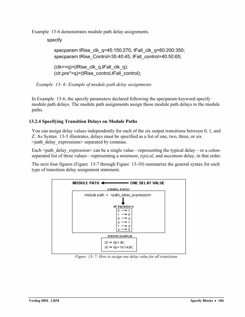
Example 13-6 demonstrates module path delay assignments.
specify
specparam tRise_clk_q=45:150:270, tFall_clk_q=60:200:350; specparam tRise_Control=35:40:45, tFall_control=40:50:65;
(clk=>q)=(tRise_clk_q,tFall_clk_q); (clr,pre*>q)=(tRise_control,tFall_control);
Example 13- 6: Example of module path delay assignments
In Example 13-6, the specify parameters declared following the specparam keyword specify module path delays. The module path assignments assign those module path delays to the module paths.
13.2.4 Specifying Transition Delays on Module Paths
You can assign delay values independently for each of the six output transitions between 0, 1, and Z. As Syntax 13-5 illustrates, delays must be specified as a list of one, two, three, or six <path_delay_expressions> separated by commas.
Each <path_delay_expression> can be a single value—representing the typical delay—or a colon-separated list of three values—representing a minimum, typical, and maximum delay, in that order.
The next four figures (Figure 13-7 through Figure 13-10) summarize the general syntax for each type of transition delay assignment statement.
Figure 13- 7: How to assign one delay value for all transitions
Verilog HDL LRM Specify Blocks • 184
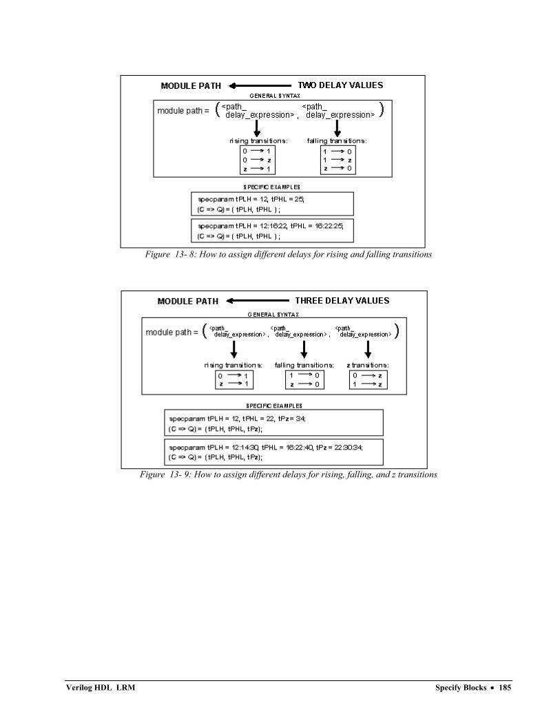
Figure 13- 8: How to assign different delays for rising and falling transitions
Figure 13- 9: How to assign different delays for rising, falling, and z transitions
Verilog HDL LRM Specify Blocks • 185
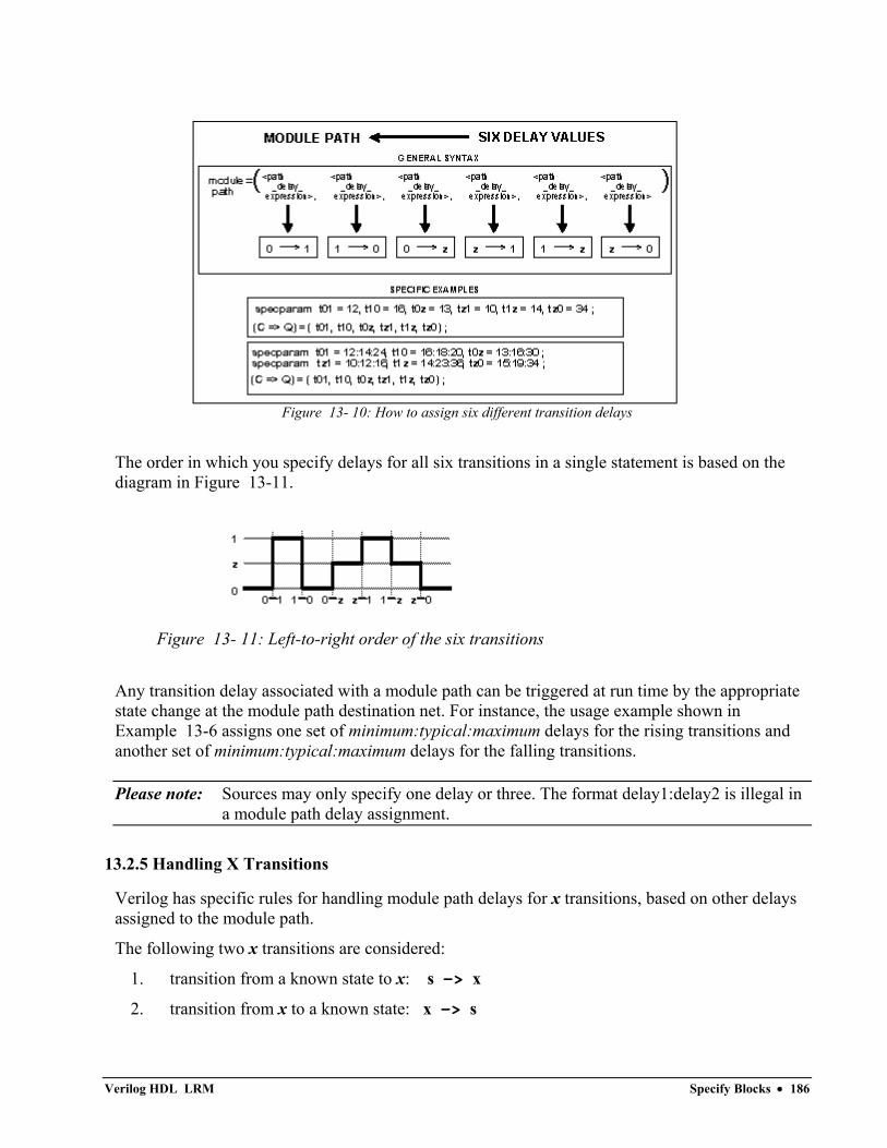
Figure 13- 10: How to assign six different transition delays
The order in which you specify delays for all six transitions in a single statement is based on the diagram in Figure 13-11.
Figure 13- 11: Left-to-right order of the six transitions
Any transition delay associated with a module path can be triggered at run time by the appropriate state change at the module path destination net. For instance, the usage example shown in Example 13-6 assigns one set of minimum:typical:maximum delays for the rising transitions and another set of minimum:typical:maximum delays for the falling transitions.
Please note: Sources may only specify one delay or three. The format delay1:delay2 is illegal in a module path delay assignment.
13.2.5 Handling X Transitions
Verilog has specific rules for handling module path delays for x transitions, based on other delays assigned to the module path.
The following two x transitions are considered:
1. transition from a known state to x: s -> x
2. transition from x to a known state: x -> s
Verilog HDL LRM Specify Blocks • 186
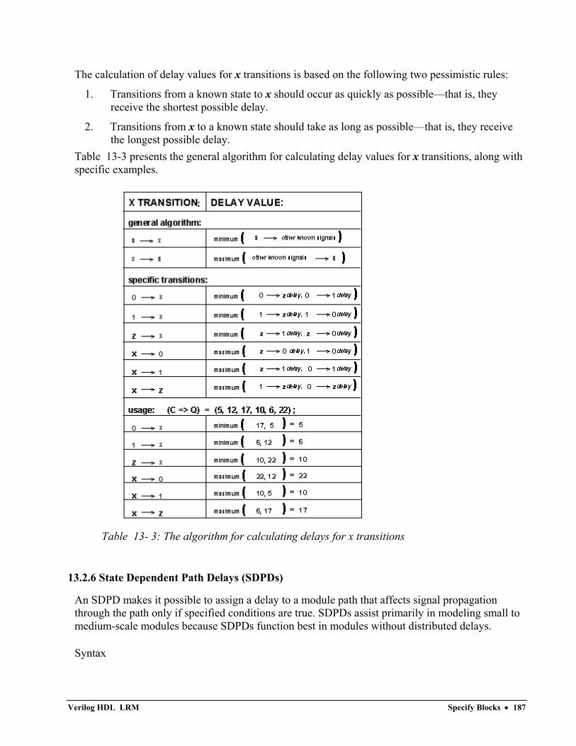
The calculation of delay values for x transitions is based on the following two pessimistic rules:
1. Transitions from a known state to x should occur as quickly as possible—that is, they receive the shortest possible delay.
2. Transitions from x to a known state should take as long as possible—that is, they receive the longest possible delay.
Table 13-3 presents the general algorithm for calculating delay values for x transitions, along with specific examples.
Table 13- 3: The algorithm for calculating delays for x transitions
13.2.6 State Dependent Path Delays (SDPDs)
An SDPD makes it possible to assign a delay to a module path that affects signal propagation through the path only if specified conditions are true. SDPDs assist primarily in modeling small to medium-scale modules because SDPDs function best in modules without distributed delays.
Syntax
Verilog HDL LRM Specify Blocks • 187
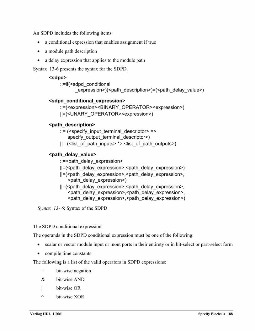
An SDPD includes the following items:
• a conditional expression that enables assignment if true
• a module path description
• a delay expression that applies to the module path
Syntax 13-6 presents the syntax for the SDPD.
<sdpd> ::=if(<sdpd_conditional
_expression>)(<path_description>)=(<path_delay_value>)
<sdpd_conditional_expression> ::=(<expression><BINARY_OPERATOR><expression>) ||=(<UNARY_OPERATOR><expression>)
<path_description> ::= (<specify_input_terminal_descriptor> =>
specify_output_terminal_descriptor>) ||= (<list_of_path_inputs> *> <list_of_path_outputs>)
<path_delay_value> ::=<path_delay_expression> ||=(<path_delay_expression>,<path_delay_expression>) ||=(<path_delay_expression>,<path_delay_expression>,
<path_delay_expression>) ||=(<path_delay_expression>,<path_delay_expression>,
<path_delay_expression>,<path_delay_expression>, <path_delay_expression>,<path_delay_expression>)
Syntax 13- 6: Syntax of the SDPD
The SDPD conditional expression
The operands in the SDPD conditional expression must be one of the following:
• scalar or vector module input or inout ports in their entirety or in bit-select or part-select form
• compile time constants
The following is a list of the valid operators in SDPD expressions:
~ bit-wise negation
& bit-wise AND
| bit-wise OR
^ bit-wise XOR
Verilog HDL LRM Specify Blocks • 188
~^ bit-wise XNOR
& reduction AND
~& reduction NAND
| reduction OR
^ reduction XOR
~^ reduction XNOR
~| reduction NOR
== logical equality
!= logical inequality
&& logical AND
|| logical OR
! logical NOT
{} concatenation
{{}} duplicate concatenation
?: conditional
An SDPD conditional expression must evaluate to one bit. The Verilog HDL treats the results X and Z as TRUE to facilitate signal propagation. The SDPD conditional expression may have any number of operands and operators.
Examples
Consider the use of an SDPD in describing an XOR in Example 13-7.
module sdpdexample (a, b, out); input a,b: output out; xor (out, a, b);
specify specparam noninvrise = 1, noninvfall = 2 specparam invertrise = 3, invertfall = 4;
Verilog HDL LRM Specify Blocks • 189
if(a) (b=>out) = (invertrise, invertfall); if(~a) (b=>out) = (noninvrise, noninvfall); if(b) (a=>out) = (invertrise,invertfall); if(~b) (a=>out) = (noninvrise,noninvfall);
endspecify endmodule
Example 13- 7: SDPD XOR example
In Example 13-7, SDPDs allow you to describe a pair of output rise and fall delay times when the XOR inverts a changing input. When the XOR buffers a changing input, SDPDs allow you to describe another pair of output rise and fall delay times.
Example 13-8 models a partial ALU. SDPDs specify different sets of path delays for different ALU operations.
`timescale 1ns / 100ps module ALU(o1, I1, I2, opcode); input [7:0] I1, i2; input [2:1] opcode; output [7:0] o1;
//functional description omitted
specify // add operation if (opcode == 2'b00) (i1,i2 *> o1) = (25.0,25.0);
// pass-through i1 operation if (opcode == 2'b01) (i1 => o1) = (5.6,8.0);
// pass-through i2 operation if (opcode == 2'b10) (i2 => o1) = (5.6,8.0);
// delays on opcode changes (opcode => o1) = (6.1,6.5); endspecify endmodule
Example 13- 8: ALU operations with different path delays
Verilog HDL LRM Specify Blocks • 190
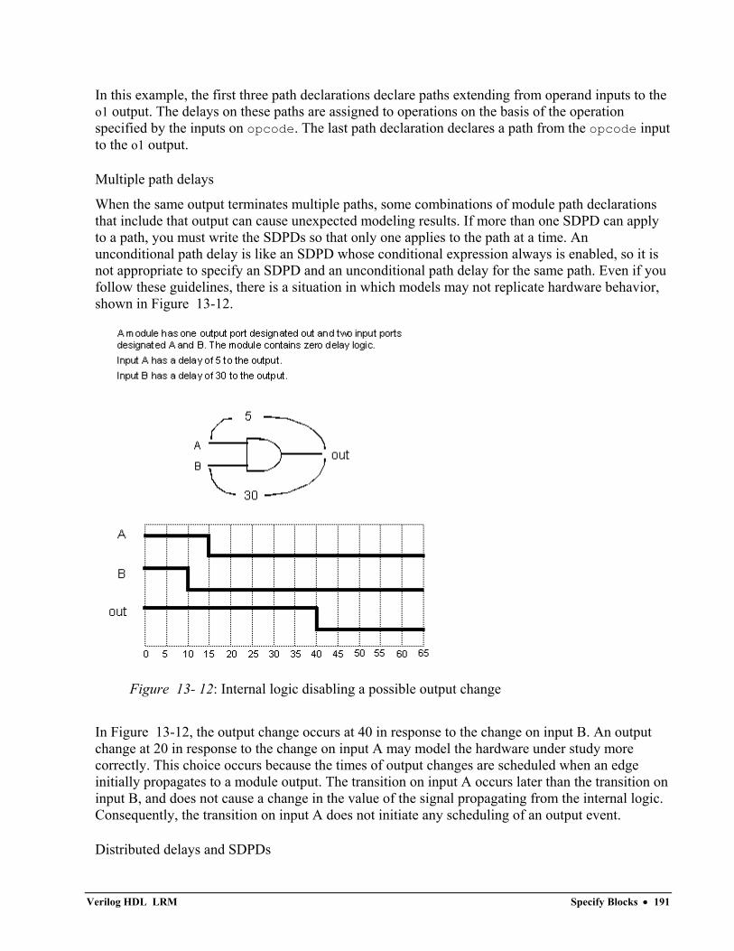
In this example, the first three path declarations declare paths extending from operand inputs to the o1 output. The delays on these paths are assigned to operations on the basis of the operation specified by the inputs on opcode. The last path declaration declares a path from the opcode input to the o1 output.
Multiple path delays
When the same output terminates multiple paths, some combinations of module path declarations that include that output can cause unexpected modeling results. If more than one SDPD can apply to a path, you must write the SDPDs so that only one applies to the path at a time. An unconditional path delay is like an SDPD whose conditional expression always is enabled, so it is not appropriate to specify an SDPD and an unconditional path delay for the same path. Even if you follow these guidelines, there is a situation in which models may not replicate hardware behavior, shown in Figure 13-12.
Figure 13- 12: Internal logic disabling a possible output change
In Figure 13-12, the output change occurs at 40 in response to the change on input B. An output change at 20 in response to the change on input A may model the hardware under study more correctly. This choice occurs because the times of output changes are scheduled when an edge initially propagates to a module output. The transition on input A occurs later than the transition on input B, and does not cause a change in the value of the signal propagating from the internal logic. Consequently, the transition on input A does not initiate any scheduling of an output event.
Distributed delays and SDPDs
Verilog HDL LRM Specify Blocks • 191

For realistic modeling, larger modules tend to necessitate gate and net delays, and behavioral models require procedural delays. These delays can have an undesirable impact on the choice of path delays, which you can avoid by following this rule:
Larger cells and modules that require distributed delays and SDPDs should meet this test: the inputs should not change before an edge generated by the most recent input change has propagated to the outputs.
This rule exists because a choice among path delays occurs when an edge initially arrives at an output, and distributed delays retard the initial arrival of the edge at an output. If the input state is a component of an SDPD conditional expression that specifies a delay for the path that the edge follows, a change in the input state before the choice of a delay can result in the choice of an inappropriate delay. The situation described in this case can also lead to output values that do not accurately model hardware.
When you apply the following pairs of delays to a path, the larger of the two delays schedules the appearance of an output change:
• a distributed delay and an unconditional delay
• a distributed delay and an SDPD
13.2.7 Driving Wired Logic
Module path output nets may not have more than one driver within the module. Therefore, wired logic is not allowed at module path outputs. Figure 13-13 and Figure 13-14 illustrate two violations of this rule.
Figure 13- 13: Illegal module paths: Two module path outputs with multiple output drivers
In Figure 13-13, any module path to Q or R is illegal.
Figure 13- 14: Illegal module paths: One module path output with multiple output drivers
Verilog HDL LRM Specify Blocks • 192
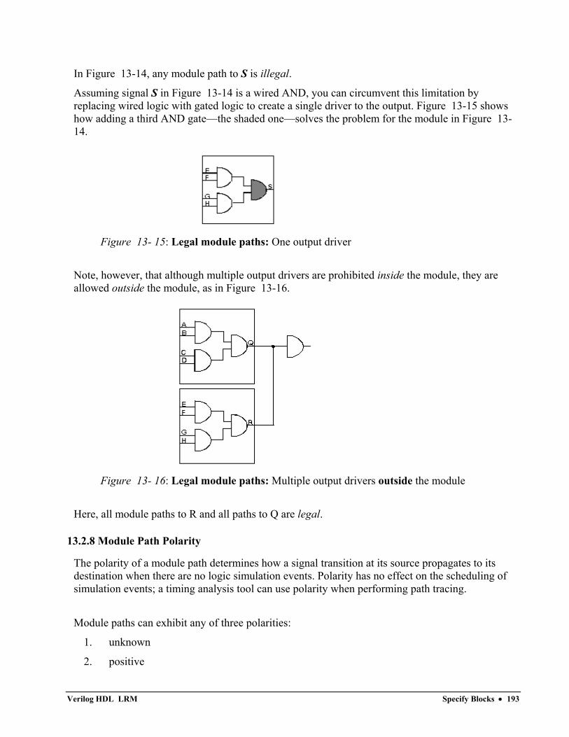
In Figure 13-14, any module path to S is illegal.
Assuming signal S in Figure 13-14 is a wired AND, you can circumvent this limitation by replacing wired logic with gated logic to create a single driver to the output. Figure 13-15 shows how adding a third AND gate—the shaded one—solves the problem for the module in Figure 13-14.
Figure 13- 15: Legal module paths: One output driver
Note, however, that although multiple output drivers are prohibited inside the module, they are allowed outside the module, as in Figure 13-16.
Figure 13- 16: Legal module paths: Multiple output drivers outside the module
Here, all module paths to R and all paths to Q are legal.
13.2.8 Module Path Polarity
The polarity of a module path determines how a signal transition at its source propagates to its destination when there are no logic simulation events. Polarity has no effect on the scheduling of simulation events; a timing analysis tool can use polarity when performing path tracing.
Module paths can exhibit any of three polarities:
1. unknown
2. positive
Verilog HDL LRM Specify Blocks • 193
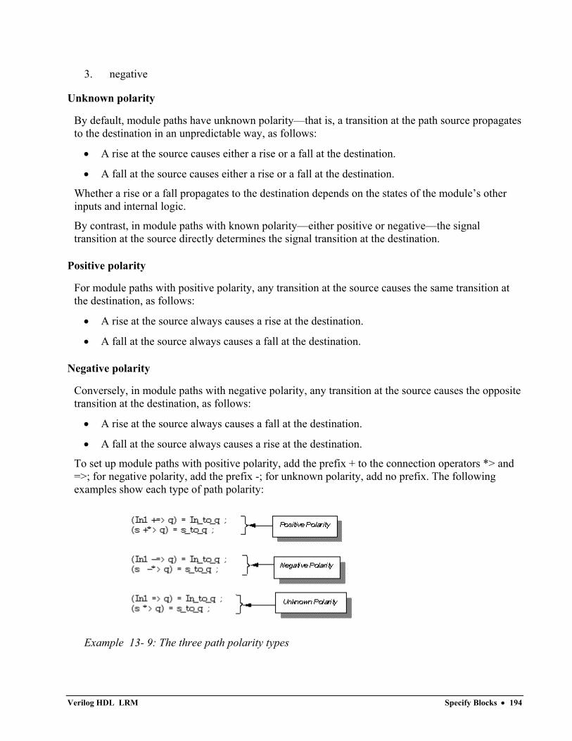
3. negative
Unknown polarity
By default, module paths have unknown polarity—that is, a transition at the path source propagates to the destination in an unpredictable way, as follows:
• A rise at the source causes either a rise or a fall at the destination.
• A fall at the source causes either a rise or a fall at the destination.
Whether a rise or a fall propagates to the destination depends on the states of the module’s other inputs and internal logic.
By contrast, in module paths with known polarity—either positive or negative—the signal transition at the source directly determines the signal transition at the destination.
Positive polarity
For module paths with positive polarity, any transition at the source causes the same transition at the destination, as follows:
• A rise at the source always causes a rise at the destination.
• A fall at the source always causes a fall at the destination.
Negative polarity
Conversely, in module paths with negative polarity, any transition at the source causes the opposite transition at the destination, as follows:
• A rise at the source always causes a fall at the destination.
• A fall at the source always causes a rise at the destination.
To set up module paths with positive polarity, add the prefix + to the connection operators *> and =>; for negative polarity, add the prefix -; for unknown polarity, add no prefix. The following examples show each type of path polarity:
Example 13- 9: The three path polarity types
Verilog HDL LRM Specify Blocks • 194
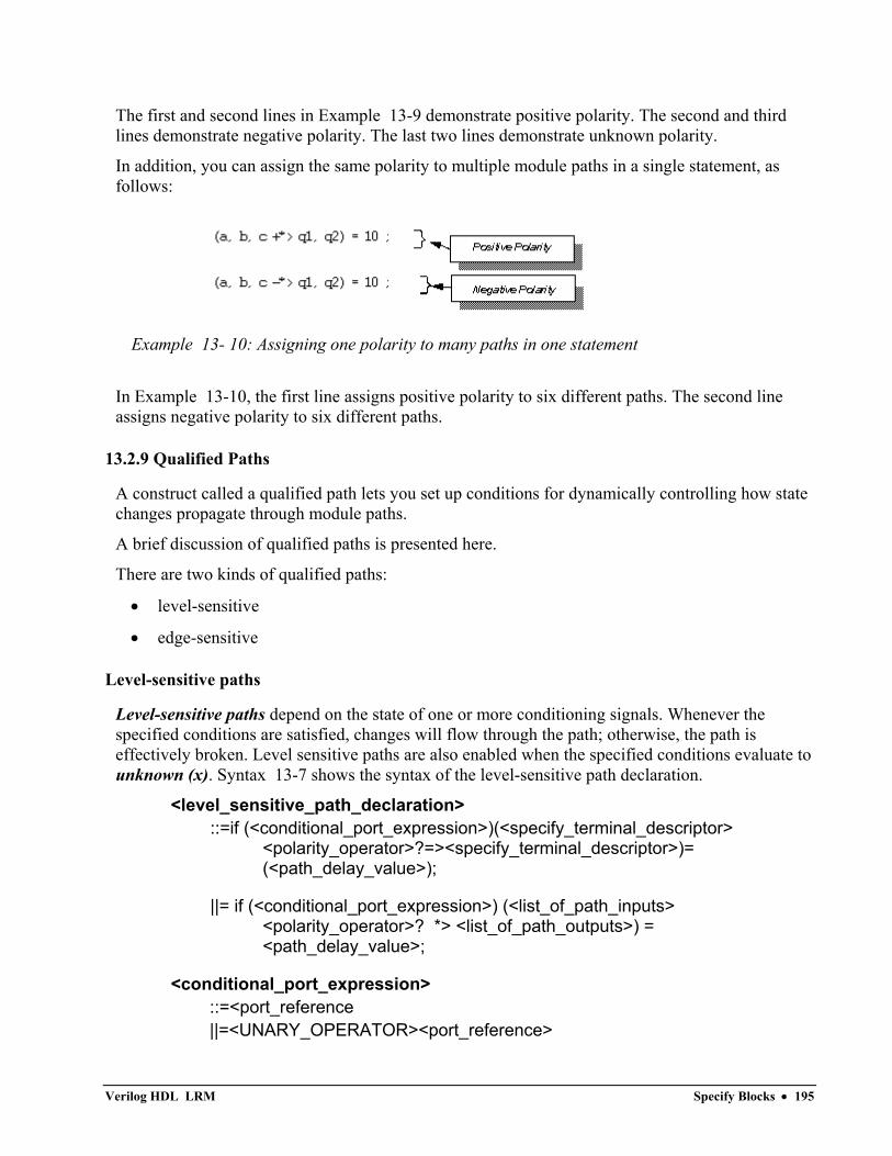
The first and second lines in Example 13-9 demonstrate positive polarity. The second and third lines demonstrate negative polarity. The last two lines demonstrate unknown polarity.
In addition, you can assign the same polarity to multiple module paths in a single statement, as follows:
Example 13- 10: Assigning one polarity to many paths in one statement
In Example 13-10, the first line assigns positive polarity to six different paths. The second line assigns negative polarity to six different paths.
13.2.9 Qualified Paths
A construct called a qualified path lets you set up conditions for dynamically controlling how state changes propagate through module paths.
A brief discussion of qualified paths is presented here.
There are two kinds of qualified paths:
• level-sensitive
• edge-sensitive
Level-sensitive paths
Level-sensitive paths depend on the state of one or more conditioning signals. Whenever the specified conditions are satisfied, changes will flow through the path; otherwise, the path is effectively broken. Level sensitive paths are also enabled when the specified conditions evaluate to unknown (x). Syntax 13-7 shows the syntax of the level-sensitive path declaration.
<level_sensitive_path_declaration> ::=if (<conditional_port_expression>)(<specify_terminal_descriptor>
<polarity_operator>?=><specify_terminal_descriptor>)= (<path_delay_value>);
||= if (<conditional_port_expression>) (<list_of_path_inputs> <polarity_operator>? *> <list_of_path_outputs>) = <path_delay_value>;
<conditional_port_expression> ::=<port_reference ||=<UNARY_OPERATOR><port_reference>
Verilog HDL LRM Specify Blocks • 195
||=<port_reference><BINARY_OPERATOR><port_reference>
Syntax 13- 7: Syntax of the level-sensitive path declaration
Verilog HDL LRM Specify Blocks • 196
Note that you can use *> for full connections or => for parallel connections. In addition, you can specify polarity and declare more than one level-sensitive path in a single statement.
Signals in the expression in Syntax 13-7 must be ports of the module that contains the path, but can be any combination of the following constructs: scalar or vector input and inout ports, or bit-selects and part-selects of those ports.
Example 13-11 demonstrates two level-sensitive path declarations without polarity operators that have the same meaning.
if (clock == 1) (in => out) = (3:4:5);
if (clock) (in => out) = (3:4:5);
Example 13- 11: Level-sensitive path declarations without polarity operators
The delay from in to out in this example will have the minimum, typical, or maximum value as selected if clock has a value of 1.
Example 13-12 demonstrates two level-sensitive path declarations with polarity operators which have the same meaning:
if (clock==0) (in+=>out) = 10;
if (!clock) (in+=>out) = 10;
Example 13- 12: Level-sensitive path declarations with polarity operators
In Example 13-12, a rise at in causes a rise at out, and a fall at in causes a fall at out. The delay from in to out is 10 if the value of clock is 0.
The following example declares multiple level-sensitive paths:
if(!clock)(in1,in2*>out1,out2)=20;
In this example, if the value of clock is 0, four paths have a delay of 20.
Implementation Specific Detail: Some tools many not allow the assignment of different delays.
Edge-sensitive paths
The other type of qualified path is edge-sensitive. In edge-sensitive paths, the path source is an edge-triggered conditioning signal. Changes flow through an edge-sensitive path when the specified edge occurs at the conditioning signal.
Syntax 13-8 shows the syntax of the edge sensitive path declaration.
<edge_sensitive_path_declaration>
Verilog HDL LRM Specify Blocks • 197
::=<if (<expression>)>? (<edge_identifier>? <specify_terminal_descriptor>=> (<specify_terminal_descriptor> <polarity_operator> ?: <data_source_expression>))=<path_delay_value>
||=<if (<expression>)>? (<edge_identifier>? <specify_terminal_descriptor> *> (<list_of_path_outputs> <polarity_operator> ?: <data_source_expression>))=<path_delay_value>
<edge_identifier> ::= posedge ||= negedge
<data_source_expression> Any expression, including constants and lists. Its width must be one bit or equal to the destination's width. If the destination is a list, the data source must be as wide as the sum of the bits of the members.
Syntax 13- 8: Syntax of the edge-sensitive path declaration
The edge-sensitive path’s edge—given in Syntax 13-8 as the <specify_terminal_descriptor> to the left of the connection operator—can be any scalar input or inout port, or bit-select of that port.
Since the edge must be one bit wide, you can specify edge-sensitive paths with full connections (*>) or parallel connections (=>), according to the rules for connection operators described in Section 13.2.1 Describing Module Paths. There are two ways to specify the path destination—the signal or signals to the left of the colon (:)—depending on the connection operator used:
• For parallel connections (=>), the destination can be any scalar output or inout port, or one of its bit-selects.
• For full connections (*>), the destination can be a list of one or more of the following signals: vector or scalar output and inout ports, and bit-selects or part-selects of those ports.
Signals in the edge-sensitive path condition given in Syntax 13-8 as the <expression> following the literal “if”—can be any scalar signals or bit-selects.
The following example demonstrates an edge-sensitive path declaration with a positive polarity operator:
( posedge clock => ( out +: in ) ) = (10, 8);
In this example, at the positive edge of clock, a module path extends from clock to out using the rise delay (10) if in is 1 and the fall delay (8) if in is 0.
The following example demonstrates an edge-sensitive path declaration with no polarity operator:
( clock => ( out : in ) ) = (10, 8);
Verilog HDL LRM Specify Blocks • 198
In this example, at any change in clock, a module path extends from clock to out using the worst case delay, which is the rise delay (10), because no polarity is specified.
The following example demonstrates an edge-sensitive path declaration with a negative polarity operator:
( negedge clock[0] => ( out -: in ) ) = (10, 8);
In this example, at the negative edge of clock[0], a module path extends from clock[0] to out using the rise delay (10) if in is 0 and the fall delay (8) if in is 1.
The following example demonstrates an edge-sensitive path declaration with a binary operation conditioning the delays:
( posedge clock*> ( ( out[0:3], out[4:7] ) +: in1 && in2 )) = (10, 8);
In this example, at the positive edge of clock, a module path extends from clock to out[0:3], and from clock to out[4:7] using the rise delay (10) if (in1 && in2) is 1, and the fall delay (8) if (in1 && in2) is 0.
The following example demonstrates an edge-sensitive path declaration preceded by a conditional expression:
if ( !reset )
(posedge clock => ( out +: in ) ) = (10, 8);
In this example, if the positive edge of clock occurs when reset is low, a module path extends from clock to out using the rise delay (10) if in is 1, and the fall delay (8) if in is 0.
Note that conditions in edge-sensitive paths are optional and need not be ports. The preceding usage example shows a condition defined with one scalar signal. In Example 13-13, a condition combines two scalars.
if ( !reset && !clear ) (posedge clock => ( out +: in ) ) = (10, 8) ;
Example 13- 13: Edge-sensitive path with three conditions
You can assign different delays to the same edge-sensitive path as long as the following criteria are met:
• The edge, condition, or both make each declaration unique.
• A signal is always referenced in the same way.
Verilog HDL LRM Specify Blocks • 199
In Example 13-14, the following four edge-sensitive path declarations are legal because each one has a unique edge or condition, all edges and data sources are specified as scalar inputs, and all destinations are specified as bit selects of a vector output.
specify (posedge clk => (q[0]:data))= (10, 5);
(negedge clk => (q[0]:data)) = (20, 12);
if (reset) (posedge clk => (q[0]:data)) = (15, 8);
if (!reset && cntrl) (posedge clk => (q[0]:data)) = (6, 2);
endspecify
Example 13- 14: Four edge-sensitive path declarations
To a timing analysis tool, the four declarations in Example 13-14 define a different set of delays for each of the four states affecting the path from clk to q[0]. However, a simulator does not care about the various states and instead uses the largest delays specified—in this case, a rise delay of 20 and a fall delay of 12.
The two declarations in Example 13-15 are not legal because even though they have different conditions, the destinations are not specified in the same way: the first destination is a part-select, the second is a bit-select.
Example 13- 15: Example of conflicting destination specifications
Verilog HDL LRM Specify Blocks • 200
Formal Syntax Definition
A.0 Syntax Overview
The following items summarize the format of the formal syntax descriptions:
1. White space may be used to separate lexical tokens.
2. Angle brackets surround each description item and are not literal symbols—that is, they do not appear in a source example of a syntax item.
3. <name> in lower case is a syntax construct item defined by other syntax construct items or by lexical token items (see next item).
4. <NAME> in upper case is a lexical token item. Its definition is a terminal node in the description hierarchy—that is, its definition does not contain any syntax construct items.
5. <name>? is an optional item.
6. <name>* is zero, one or more items.
7. <name>+ is one or more items.
8. <name> <,<name>>* is a comma-separated list of items with at least one item in the list.
9. if [condition] is a condition placed on one of several definitions
10. <name> ::= gives a syntax definition to an item.
11. ||= introduces an alternative syntax definition.
12. name is a literal (a keyword). For example, the definition <event_declaration> ::= event <name_of_event> stipulates that the keyword “event” precedes the name of an event in an event declaration.
13. ( . . . ) places parenthesis symbols in a definition. These parentheses are literals required by the syntax being defined. Other literal symbols can also appear in a definition (for example, . and :).
Please note: In Verilog syntax, a period (.) may not be preceded or followed by a space.
A.1 Source Text
<source_text> ::= <description>*
<description> ::= <module> ||= <primitive>
<module> ::= module <name_of_module> <list_of_ports>? ;
<module_item>* endmodule
Verilog HDL LRM Formal Syntax Definition • 201
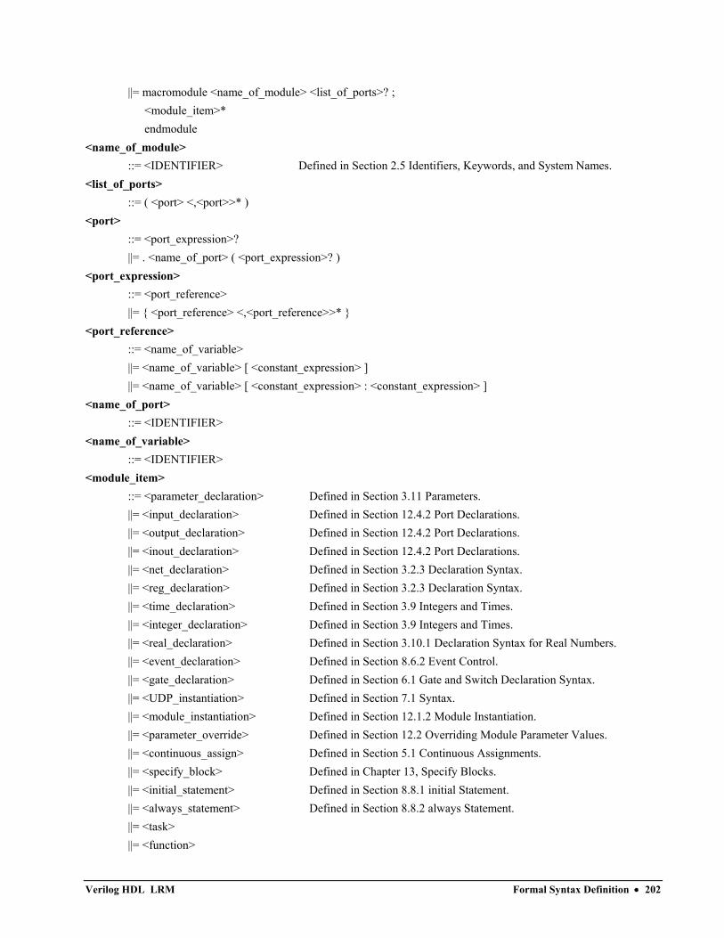
||= macromodule <name_of_module> <list_of_ports>? ; <module_item>* endmodule
<name_of_module> ::= <IDENTIFIER> Defined in Section 2.5 Identifiers, Keywords, and System Names.
<list_of_ports> ::= ( <port> <,<port>>* )
<port> ::= <port_expression>? ||= . <name_of_port> ( <port_expression>? )
<port_expression> ::= <port_reference> ||= { <port_reference> <,<port_reference>>* }
<port_reference> ::= <name_of_variable> ||= <name_of_variable> [ <constant_expression> ] ||= <name_of_variable> [ <constant_expression> : <constant_expression> ]
<name_of_port> ::= <IDENTIFIER>
<name_of_variable> ::= <IDENTIFIER>
<module_item> ::= <parameter_declaration> Defined in Section 3.11 Parameters. ||= <input_declaration> Defined in Section 12.4.2 Port Declarations. ||= <output_declaration> Defined in Section 12.4.2 Port Declarations. ||= <inout_declaration> Defined in Section 12.4.2 Port Declarations. ||= <net_declaration> Defined in Section 3.2.3 Declaration Syntax. ||= <reg_declaration> Defined in Section 3.2.3 Declaration Syntax. ||= <time_declaration> Defined in Section 3.9 Integers and Times. ||= <integer_declaration> Defined in Section 3.9 Integers and Times. ||= <real_declaration> Defined in Section 3.10.1 Declaration Syntax for Real Numbers. ||= <event_declaration> Defined in Section 8.6.2 Event Control. ||= <gate_declaration> Defined in Section 6.1 Gate and Switch Declaration Syntax. ||= <UDP_instantiation> Defined in Section 7.1 Syntax. ||= <module_instantiation> Defined in Section 12.1.2 Module Instantiation. ||= <parameter_override> Defined in Section 12.2 Overriding Module Parameter Values. ||= <continuous_assign> Defined in Section 5.1 Continuous Assignments. ||= <specify_block> Defined in Chapter 13, Specify Blocks. ||= <initial_statement> Defined in Section 8.8.1 initial Statement. ||= <always_statement> Defined in Section 8.8.2 always Statement. ||= <task> ||= <function>
Verilog HDL LRM Formal Syntax Definition • 202
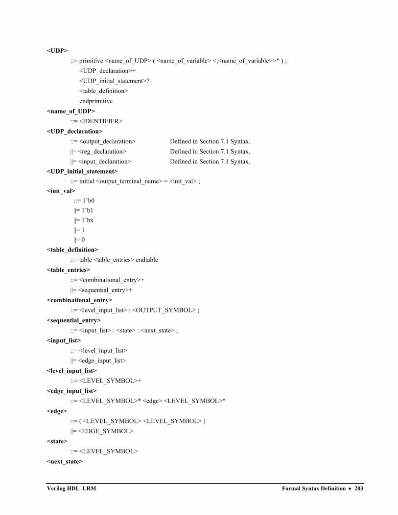
<UDP> ::= primitive <name_of_UDP> ( <name_of_variable> <,<name_of_variable>>* ) ;
<UDP_declaration>+ <UDP_initial_statement>? <table_definition> endprimitive
<name_of_UDP> ::= <IDENTIFIER>
<UDP_declaration> ::= <output_declaration> Defined in Section 7.1 Syntax. ||= <reg_declaration> Defined in Section 7.1 Syntax. ||= <input_declaration> Defined in Section 7.1 Syntax.
<UDP_initial_statement> ::= initial <output_terminal_name> = <init_val> ;
<init_val> ::= 1’b0 ||= 1’b1 ||= 1’bx ||= 1 ||= 0
<table_definition> ::= table <table_entries> endtable
<table_entries> ::= <combinational_entry>+ ||= <sequential_entry>+
<combinational_entry> ::= <level_input_list> : <OUTPUT_SYMBOL> ;
<sequential_entry> ::= <input_list> : <state> : <next_state> ;
<input_list> ::= <level_input_list> ||= <edge_input_list>
<level_input_list> ::= <LEVEL_SYMBOL>+
<edge_input_list> ::= <LEVEL_SYMBOL>* <edge> <LEVEL_SYMBOL>*
<edge> ::= ( <LEVEL_SYMBOL> <LEVEL_SYMBOL> ) ||= <EDGE_SYMBOL>
<state> ::= <LEVEL_SYMBOL>
<next_state>
Verilog HDL LRM Formal Syntax Definition • 203
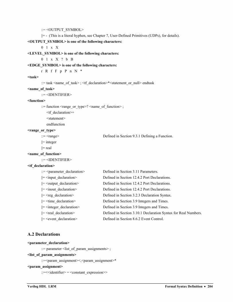
::= <OUTPUT_SYMBOL> ||= - (This is a literal hyphen, see Chapter 7, User-Defined Primitives (UDPs), for details).
<OUTPUT_SYMBOL> is one of the following characters: 0 1 x X
<LEVEL_SYMBOL> is one of the following characters: 0 1 x X ? b B
<EDGE_SYMBOL> is one of the following characters: r R f F p P n N *
<task> ::= task <name_of_task> ; <tf_declaration>*<statement_or_null> endtask
<name_of_task> ::= <IDENTIFIER>
<function> ::= function <range_or_type>? <name_of_function> ;
<tf_declaration>+ <statement> endfunction
<range_or_type> ::= <range> Defined in Section 9.3.1 Defining a Function. ||= integer ||= real
<name_of_function> ::= <IDENTIFIER>
<tf_declaration> ::= <parameter_declaration> Defined in Section 3.11 Parameters. ||= <input_declaration> Defined in Section 12.4.2 Port Declarations. ||= <output_declaration> Defined in Section 12.4.2 Port Declarations. ||= <inout_declaration> Defined in Section 12.4.2 Port Declarations. ||= <reg_declaration> Defined in Section 3.2.3 Declaration Syntax. ||= <time_declaration> Defined in Section 3.9 Integers and Times. ||= <integer_declaration> Defined in Section 3.9 Integers and Times. ||= <real_declaration> Defined in Section 3.10.1 Declaration Syntax for Real Numbers. ||= <event_declaration> Defined in Section 8.6.2 Event Control.
A.2 Declarations
<parameter_declaration> ::= parameter <list_of_param_assignments> ;
<list_of_param_assignments> ::=<param_assignment><,<param_assignment>*
<param_assignment> ::=<<identifier> = <constant_expression>>
Verilog HDL LRM Formal Syntax Definition • 204
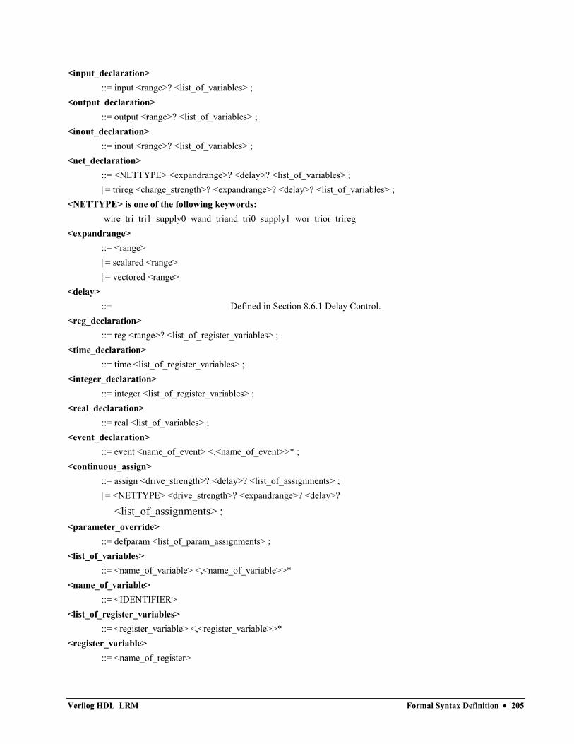
<input_declaration> ::= input <range>? <list_of_variables> ;
<output_declaration> ::= output <range>? <list_of_variables> ;
<inout_declaration> ::= inout <range>? <list_of_variables> ;
<net_declaration> ::= <NETTYPE> <expandrange>? <delay>? <list_of_variables> ; ||= trireg <charge_strength>? <expandrange>? <delay>? <list_of_variables> ;
<NETTYPE> is one of the following keywords: wire tri tri1 supply0 wand triand tri0 supply1 wor trior trireg
<expandrange> ::= <range> ||= scalared <range> ||= vectored <range>
<delay> ::= Defined in Section 8.6.1 Delay Control.
<reg_declaration> ::= reg <range>? <list_of_register_variables> ;
<time_declaration> ::= time <list_of_register_variables> ;
<integer_declaration> ::= integer <list_of_register_variables> ;
<real_declaration> ::= real <list_of_variables> ;
<event_declaration> ::= event <name_of_event> <,<name_of_event>>* ;
<continuous_assign> ::= assign <drive_strength>? <delay>? <list_of_assignments> ; ||= <NETTYPE> <drive_strength>? <expandrange>? <delay>?
<list_of_assignments> ; <parameter_override>
::= defparam <list_of_param_assignments> ; <list_of_variables>
::= <name_of_variable> <,<name_of_variable>>* <name_of_variable>
::= <IDENTIFIER> <list_of_register_variables>
::= <register_variable> <,<register_variable>>* <register_variable>
::= <name_of_register>
Verilog HDL LRM Formal Syntax Definition • 205
||= <name_of_memory> [ <constant_expression> : <constant_expression> ] <constant_expression>
::= Defined in Chapter 4,Expressions. <name_of_register> ::= <IDENTIFIER> Defined in Section 2.5 Identifiers, Keywords, and System Names. <name_of_memory> ::= <IDENTIFIER> Defined in Section 2.5 Identifiers, Keywords, and System Names. <name_of_event> ::= <IDENTIFIER> Defined in Section 2.5 Identifiers, Keywords, and System Names.
<charge_strength> ::= ( small ) ||= ( medium ) ||= ( large )
<drive_strength> ::= ( <STRENGTH0> , <STRENGTH1> ) ||= ( <STRENGTH1> , <STRENGTH0> )
<STRENGTH0> is one of the following keywords: supply0 strong0 pull0 weak0 highz0
<STRENGTH1> is one of the following keywords: supply1 strong1 pull1 weak1 highz1
<range> ::= [ <constant_expression> : <constant_expression> ]
<list_of_assignments> ::= <assignment> <,<assignment>>*
<expression> ::= Defined in Chapter 4, Expressions.
<assignment> ::= Defined in Chapter 8, 8.2 Procedural Assignments.
A.3 Primitive instances
<gate_declaration> ::= <GATETYPE> <drive_strength>? <delay>? <gate_instance>
<,<gate_instance>>* ; <GATETYPE> is one of the following keywords:
and nand or nor xor xnor buf bufif0 bufif1 not notif0 notif1 pulldown pullup nmos rnmos pmos rpmos cmos rcmos tran rtran tranif0 rtranif0 tranif1 rtranif1
<drive_strength> ::= (<STRENGTH0>,<STRENGTH1>) ||=(<STRENGTH1>,<STRENGTH0>)
<delay> ::= # <number>
Verilog HDL LRM Formal Syntax Definition • 206
||= # <identifier> ||= # (<mintypmax_expression> <,<mintypmax_expression>>?
<,<mintypmax_expression>>?) <gate_instance>
::= <name_of_gate_instance>? ( <terminal> <,<terminal>>* ) <name_of_gate_instance>
::= <IDENTIFIER> Defined in Section 2.5 Identifiers, Keywords, and System Names. <UDP_instantiation>
::= <name_of_UDP> <drive_strength>? <delay>? <UDP_instance>
<,<UDP_instance>>* ; <name_of_UDP>
::= <IDENTIFIER> Defined in Section 2.5 Identifiers, Keywords, and System Names. <UDP_instance>
::= <name_of_UDP_instance>? ( <terminal> <,<terminal>>* ) <name_of_UDP_instance>
::= <IDENTIFIER> Defined in Section 2.5 Identifiers, Keywords, and System Names. <terminal>
::= <expression> ||= <IDENTIFIER>
A.4 Module Instantiations
<module_instantiation> ::= <name_of_module> <parameter_value_assignment>?
<module_instance> <,<module_instance>>* ; <name_of_module>
::= <IDENTIFIER> Defined in Section 2.5 Identifiers, Keywords, and System Names. <parameter_value_assignment>
::= # ( <expression> <,<expression>>* ) <module_instance>
::= <name_of_instance> ( <list_of_module_connections>? ) <name_of_instance>
::= <IDENTIFIER> Defined in Section 2.5 Identifiers, Keywords, and System Names. <list_of_module_connections>
::= <module_port_connection> <,<module_port_connection>>* ||= <named_port_connection> <,<named_port_connection>>*
<module_port_connection> ::= <expression> Defined in Chapter 4, Expressions. ||= <NULL>
<NULL> ::= nothing—this form covers the case of an empty item in a list—for example: (a, b, , d)
Verilog HDL LRM Formal Syntax Definition • 207
<named_port_connection> ::= .< IDENTIFIER> ( <expression> )
<expression> ::= Defined in Chapter 4, Expressions.
A.5 Behavioral Statements
<initial_statement> ::= initial <statement>
<always_statement> ::= always <statement>
<statement_or_null> ::= <statement> ||= ;
<statement> ::=<blocking assignment> ; ||= <non-blocking assignment> ; ||= if ( <expression> ) <statement_or_null> ||= if ( <expression> ) <statement_or_null>
else <statement_or_null> ||= case ( <expression> ) <case_item>+ endcase ||= casez ( <expression> ) <case_item>+ endcase ||= casex ( <expression> ) <case_item>+ endcase ||= forever <statement> ||= repeat ( <expression> ) <statement> ||= while ( <expression> ) <statement> ||= for ( <assignment> ; <expression> ; <assignment> )
<statement> ||= <delay_control> <statement_or_null> Defined in Section 8.6.1 Delay Control. ||= <event_control> <statement_or_null> Defined in Section 8.6.2 Event Control. ||= wait ( <expression> ) <statement_or_null> ||= -> <name_of_event> ; ||= <seq_block> ||= <par_block> ||= <task_enable> ||= <system_task_enable> ||= disable <name_of_task> ; ||= disable <name_of_block> ; ||= force <assignment> ; ||= release <lvalue> ;
<assignment>
Verilog HDL LRM Formal Syntax Definition • 208
::= <lvalue> = <expression> <blocking assignment>
::= <lvalue> = <expression> ||= <lvalue> = <delay_control> <expression> ; ||= <lvalue> = <event_control> <expression> ;
<non-blocking assignment> ::= <lvalue> <= <expression> ||= <lvalue> <= <delay_control> <expression> ; ||= <lvalue> <= <event_control> <expression> ;
<lvalue> ::= Defined in Section 8.2 Procedural Assignments.
<expression> ::= Defined in Chapter 4, Expressions.
<case_item> ::= <expression> <,<expression>>* : <statement_or_null> ||= default : <statement_or_null> ||= default <statement_or_null>
<seq_block> ::= begin <statement>* end ||= begin : <name_of_block> <block_declaration>* <statement>* end
<par_block> ::= fork <statement>* join ||= fork : <name_of_block> <block_declaration>* <statement>* join
<name_of_block> ::= <IDENTIFIER>
<block_declaration> ::= <parameter_declaration> Defined in Section 3.11 Parameters. ||= <reg_declaration> Defined in Section 3.2.3 Declaration Syntax. ||= <integer_declaration> Defined in Section 3.9 Integers and Times. ||= <real_declaration> Defined in Section 3.10 Real Numbers. ||= <time_declaration> Defined in Section 3.9 Integers and Times. ||= <event_declaration> Defined in Section 8.6.2 Event Control.
<task_enable> ::= <name_of_task> ; Defined in Section 9.2.1 Defining a Task. ||= <name_of_task> ( <expression> <,<expression>>* ) ;
<system_task_enable> ::= <name_of_system_task> ; ||= <name_of_system_task> ( <expression> <,<expression>>* ) ;
<name_of_system_task> ::= $<SYSTEM_IDENTIFIER>
Please note: The $ may not be followed by a space.
Verilog HDL LRM Formal Syntax Definition • 209
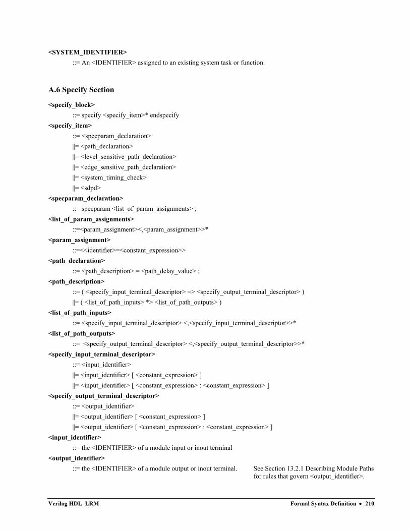
<SYSTEM_IDENTIFIER> ::= An <IDENTIFIER> assigned to an existing system task or function.
A.6 Specify Section
<specify_block> ::= specify <specify_item>* endspecify
<specify_item> ::= <specparam_declaration> ||= <path_declaration> ||= <level_sensitive_path_declaration> ||= <edge_sensitive_path_declaration> ||= <system_timing_check> ||= <sdpd>
<specparam_declaration> ::= specparam <list_of_param_assignments> ;
<list_of_param_assignments> ::=<param_assignment><,<param_assignment>>*
<param_assignment> ::=<<identifier>=<constant_expression>>
<path_declaration> ::= <path_description> = <path_delay_value> ;
<path_description> ::= ( <specify_input_terminal_descriptor> => <specify_output_terminal_descriptor> ) ||= ( <list_of_path_inputs> *> <list_of_path_outputs> )
<list_of_path_inputs> ::= <specify_input_terminal_descriptor> <,<specify_input_terminal_descriptor>>*
<list_of_path_outputs> ::= <specify_output_terminal_descriptor> <,<specify_output_terminal_descriptor>>*
<specify_input_terminal_descriptor> ::= <input_identifier> ||= <input_identifier> [ <constant_expression> ] ||= <input_identifier> [ <constant_expression> : <constant_expression> ]
<specify_output_terminal_descriptor> ::= <output_identifier> ||= <output_identifier> [ <constant_expression> ] ||= <output_identifier> [ <constant_expression> : <constant_expression> ]
<input_identifier> ::= the <IDENTIFIER> of a module input or inout terminal
<output_identifier> ::= the <IDENTIFIER> of a module output or inout terminal. See Section 13.2.1 Describing Module Paths
for rules that govern <output_identifier>.
Verilog HDL LRM Formal Syntax Definition • 210
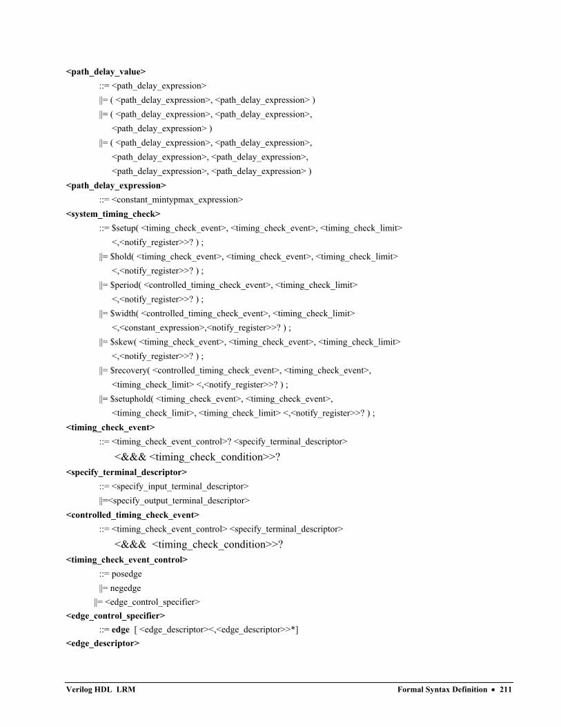
<path_delay_value> ::= <path_delay_expression> ||= ( <path_delay_expression>, <path_delay_expression> ) ||= ( <path_delay_expression>, <path_delay_expression>,
<path_delay_expression> ) ||= ( <path_delay_expression>, <path_delay_expression>,
<path_delay_expression>, <path_delay_expression>, <path_delay_expression>, <path_delay_expression> )
<path_delay_expression> ::= <constant_mintypmax_expression>
<system_timing_check> ::= $setup( <timing_check_event>, <timing_check_event>, <timing_check_limit>
<,<notify_register>>? ) ; ||= $hold( <timing_check_event>, <timing_check_event>, <timing_check_limit>
<,<notify_register>>? ) ; ||= $period( <controlled_timing_check_event>, <timing_check_limit>
<,<notify_register>>? ) ; ||= $width( <controlled_timing_check_event>, <timing_check_limit>
<,<constant_expression>,<notify_register>>? ) ; ||= $skew( <timing_check_event>, <timing_check_event>, <timing_check_limit>
<,<notify_register>>? ) ; ||= $recovery( <controlled_timing_check_event>, <timing_check_event>,
<timing_check_limit> <,<notify_register>>? ) ; ||= $setuphold( <timing_check_event>, <timing_check_event>,
<timing_check_limit>, <timing_check_limit> <,<notify_register>>? ) ; <timing_check_event>
::= <timing_check_event_control>? <specify_terminal_descriptor>
<&&& <timing_check_condition>>? <specify_terminal_descriptor>
::= <specify_input_terminal_descriptor> ||=<specify_output_terminal_descriptor>
<controlled_timing_check_event> ::= <timing_check_event_control> <specify_terminal_descriptor>
<&&& <timing_check_condition>>? <timing_check_event_control>
::= posedge ||= negedge
||= <edge_control_specifier> <edge_control_specifier>
::= edge [ <edge_descriptor><,<edge_descriptor>>*] <edge_descriptor>
Verilog HDL LRM Formal Syntax Definition • 211
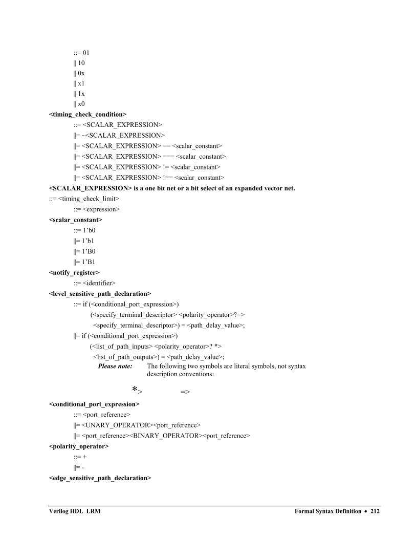
::= 01 || 10 || 0x || x1 || 1x || x0 <timing_check_condition>
::= <SCALAR_EXPRESSION> ||= ~<SCALAR_EXPRESSION> ||= <SCALAR_EXPRESSION> == <scalar_constant> ||= <SCALAR_EXPRESSION> === <scalar_constant> ||= <SCALAR_EXPRESSION> != <scalar_constant> ||= <SCALAR_EXPRESSION> !== <scalar_constant>
<SCALAR_EXPRESSION> is a one bit net or a bit select of an expanded vector net. ::= <timing_check_limit>
::= <expression> <scalar_constant>
::= 1’b0 ||= 1’b1 ||= 1’B0 ||= 1’B1
<notify_register> ::= <identifier>
<level_sensitive_path_declaration> ::= if (<conditional_port_expression>)
(<specify_terminal_descriptor> <polarity_operator>?=> <specify_terminal_descriptor>) = <path_delay_value>;
||= if (<conditional_port_expression>) (<list_of_path_inputs> <polarity_operator>? *> <list_of_path_outputs>) = <path_delay_value>;
Please note: The following two symbols are literal symbols, not syntax description conventions:
*> => <conditional_port_expression>
::= <port_reference> ||= <UNARY_OPERATOR><port_reference> ||= <port_reference><BINARY_OPERATOR><port_reference>
<polarity_operator> ::= + ||= -
<edge_sensitive_path_declaration>
Verilog HDL LRM Formal Syntax Definition • 212
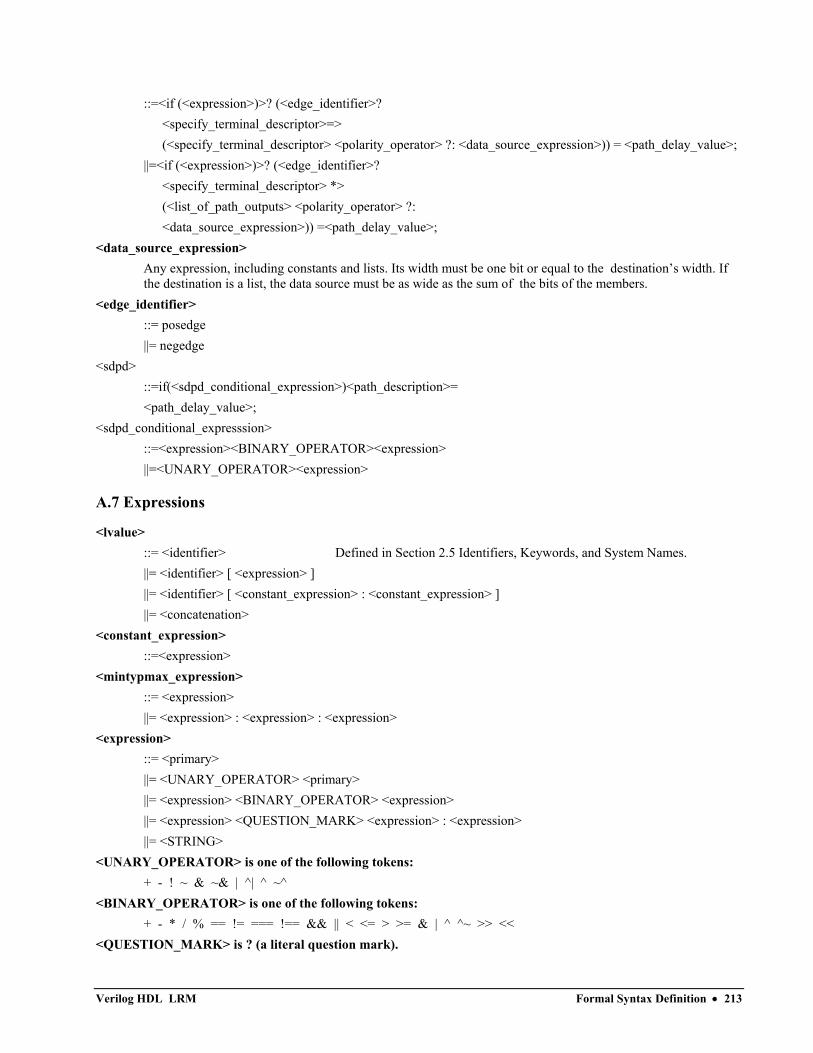
::=<if (<expression>)>? (<edge_identifier>? <specify_terminal_descriptor>=> (<specify_terminal_descriptor> <polarity_operator> ?: <data_source_expression>)) = <path_delay_value>;
||=<if (<expression>)>? (<edge_identifier>? <specify_terminal_descriptor> *> (<list_of_path_outputs> <polarity_operator> ?: <data_source_expression>)) =<path_delay_value>;
<data_source_expression> Any expression, including constants and lists. Its width must be one bit or equal to the destination’s width. If the destination is a list, the data source must be as wide as the sum of the bits of the members.
<edge_identifier> ::= posedge ||= negedge
<sdpd> ::=if(<sdpd_conditional_expression>)<path_description>= <path_delay_value>;
<sdpd_conditional_expresssion> ::=<expression><BINARY_OPERATOR><expression> ||=<UNARY_OPERATOR><expression>
A.7 Expressions
<lvalue> ::= <identifier> Defined in Section 2.5 Identifiers, Keywords, and System Names. ||= <identifier> [ <expression> ] ||= <identifier> [ <constant_expression> : <constant_expression> ] ||= <concatenation>
<constant_expression> ::=<expression>
<mintypmax_expression> ::= <expression> ||= <expression> : <expression> : <expression>
<expression> ::= <primary> ||= <UNARY_OPERATOR> <primary> ||= <expression> <BINARY_OPERATOR> <expression> ||= <expression> <QUESTION_MARK> <expression> : <expression> ||= <STRING>
<UNARY_OPERATOR> is one of the following tokens: + - ! ~ & ~& | ^| ^ ~^
<BINARY_OPERATOR> is one of the following tokens: + - * / % == != === !== && || < <= > >= & | ^ ^~ >> <<
<QUESTION_MARK> is ? (a literal question mark).
Verilog HDL LRM Formal Syntax Definition • 213
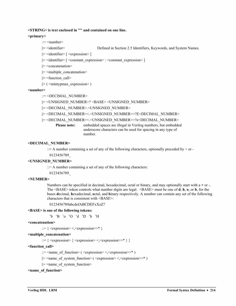
<STRING> is text enclosed in "" and contained on one line. <primary>
::= <number> ||= <identifier> Defined in Section 2.5 Identifiers, Keywords, and System Names. ||= <identifier> [ <expression> ] ||= <identifier> [ <constant_expression> : <constant_expression> ] ||= <concatenation> ||= <multiple_concatenation> ||= <function_call> ||= ( <mintypmax_expression> )
<number> ::= <DECIMAL_NUMBER> ||= <UNSIGNED_NUMBER>? <BASE> <UNSIGNED_NUMBER> ||= <DECIMAL_NUMBER>.<UNSIGNED_NUMBER> ||= <DECIMAL_NUMBER><.<UNSIGNED_NUMBER>>?E<DECIMAL_NUMBER> ||= <DECIMAL_NUMBER><.<UNSIGNED_NUMBER>>?e<DECIMAL_NUMBER>
Please note: embedded spaces are illegal in Verilog numbers, but embedded underscore characters can be used for spacing in any type of number.
<DECIMAL_NUMBER> ::= A number containing a set of any of the following characters, optionally preceded by + or -
0123456789_ <UNSIGNED_NUMBER>
::= A number containing a set of any of the following characters: 0123456789_
<NUMBER> Numbers can be specified in decimal, hexadecimal, octal or binary, and may optionally start with a + or -. The <BASE> token controls what number digits are legal. <BASE> must be one of d, h, o, or b, for the bases decimal, hexadecimal, octal, and binary respectively. A number can contain any set of the following characters that is consistent with <BASE>:
0123456789abcdefABCDEFxXzZ? <BASE> is one of the following tokens:
’b ’B ’o ’O ’d ’D ’h ’H <concatenation>
::= { <expression> <,<expression>>* } <multiple_concatenation>
::= { <expression> { <expression> <,<expression>>* } } <function_call>
::= <name_of_function> ( <expression> <,<expression>>* ) ||= <name_of_system_function> ( <expression> <,<expression>>* ) ||= <name_of_system_function>
<name_of_function>
Verilog HDL LRM Formal Syntax Definition • 214
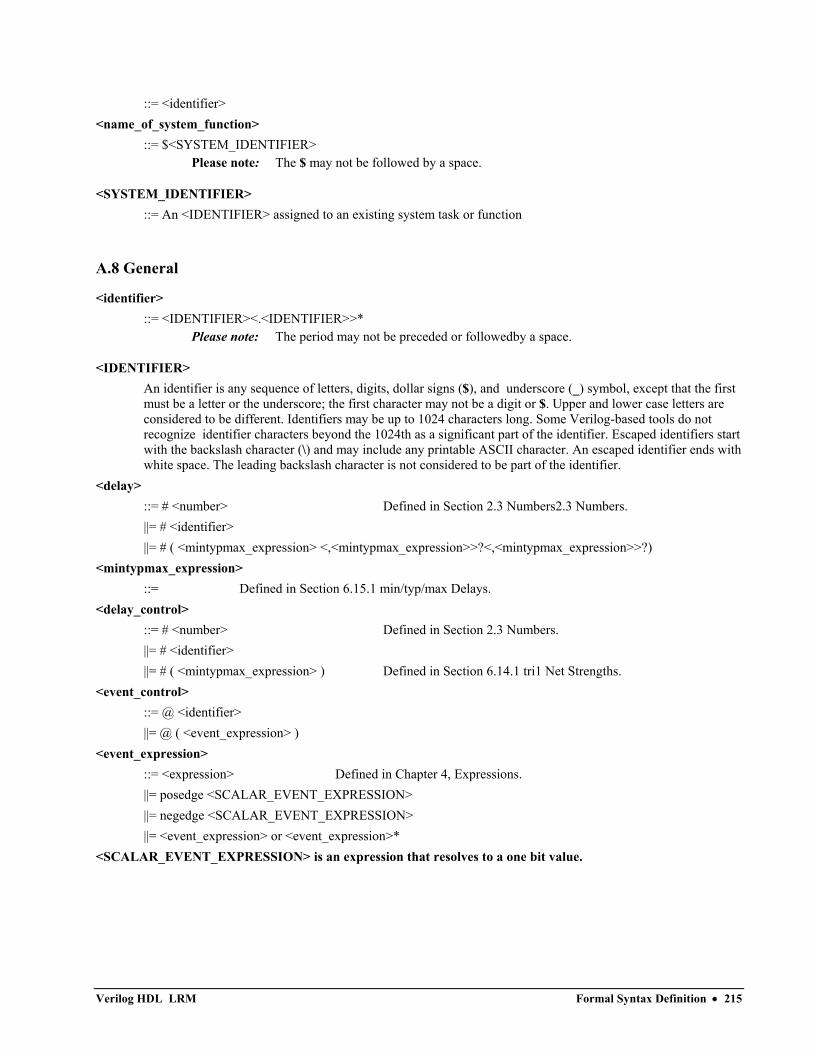
::= <identifier> <name_of_system_function>
::= $<SYSTEM_IDENTIFIER> Please note: The $ may not be followed by a space.
<SYSTEM_IDENTIFIER> ::= An <IDENTIFIER> assigned to an existing system task or function
A.8 General
<identifier> ::= <IDENTIFIER><.<IDENTIFIER>>*
Please note: The period may not be preceded or followedby a space.
<IDENTIFIER> An identifier is any sequence of letters, digits, dollar signs ($), and underscore (_) symbol, except that the first must be a letter or the underscore; the first character may not be a digit or $. Upper and lower case letters are considered to be different. Identifiers may be up to 1024 characters long. Some Verilog-based tools do not recognize identifier characters beyond the 1024th as a significant part of the identifier. Escaped identifiers start with the backslash character (\) and may include any printable ASCII character. An escaped identifier ends with white space. The leading backslash character is not considered to be part of the identifier.
<delay> ::= # <number> Defined in Section 2.3 Numbers2.3 Numbers. ||= # <identifier> ||= # ( <mintypmax_expression> <,<mintypmax_expression>>?<,<mintypmax_expression>>?)
<mintypmax_expression> ::= Defined in Section 6.15.1 min/typ/max Delays.
<delay_control> ::= # <number> Defined in Section 2.3 Numbers. ||= # <identifier> ||= # ( <mintypmax_expression> ) Defined in Section 6.14.1 tri1 Net Strengths.
<event_control> ::= @ <identifier> ||= @ ( <event_expression> )
<event_expression> ::= <expression> Defined in Chapter 4, Expressions. ||= posedge <SCALAR_EVENT_EXPRESSION> ||= negedge <SCALAR_EVENT_EXPRESSION> ||= <event_expression> or <event_expression>*
<SCALAR_EVENT_EXPRESSION> is an expression that resolves to a one bit value.
Verilog HDL LRM Formal Syntax Definition • 215
System Tasks and Functions
B.0 System Tasks Overview
This section describes system tasks and functions that are tool implementation specific.
Below is a list of the tasks and functions described. For the function marked with an asterisk, the host machine native arithmetic is used.
$bitstoreal $rtoi
$display $setup
$finish $skew
$hold $setuphold
$itor $strobe
$period $time
$printtimescale $timeformat
$realtime $width
$realtobits $write
$recovery
These utility tasks and functions provide some broadly useful capabilities. The following sections describe the behavior of these tasks and functions—without giving the complete implementation details.
B.1 The Display and Write Tasks
Syntax: $display(P1, P2, ... , Pn);
$write(P1, P2, ... , Pn);
These are the main system task routines for displaying information. The two tasks are identical except that $display automatically adds a newline character to the end of its output, whereas the $write task does not. Thus, if you want to print several messages on a single line, you should use the $write task.
The $display and $write tasks display their parameters in the same order they appear in the parameter list. Each parameter can be a quoted string, an expression that returns a value, or a null parameter.
The contents of string parameters are output literally except when certain escape sequences are inserted to display special characters or specify the display format for a subsequent expression.
Escape sequences are inserted into a string in three ways:
Verilog HDL LRM System Tasks and Functions • 216
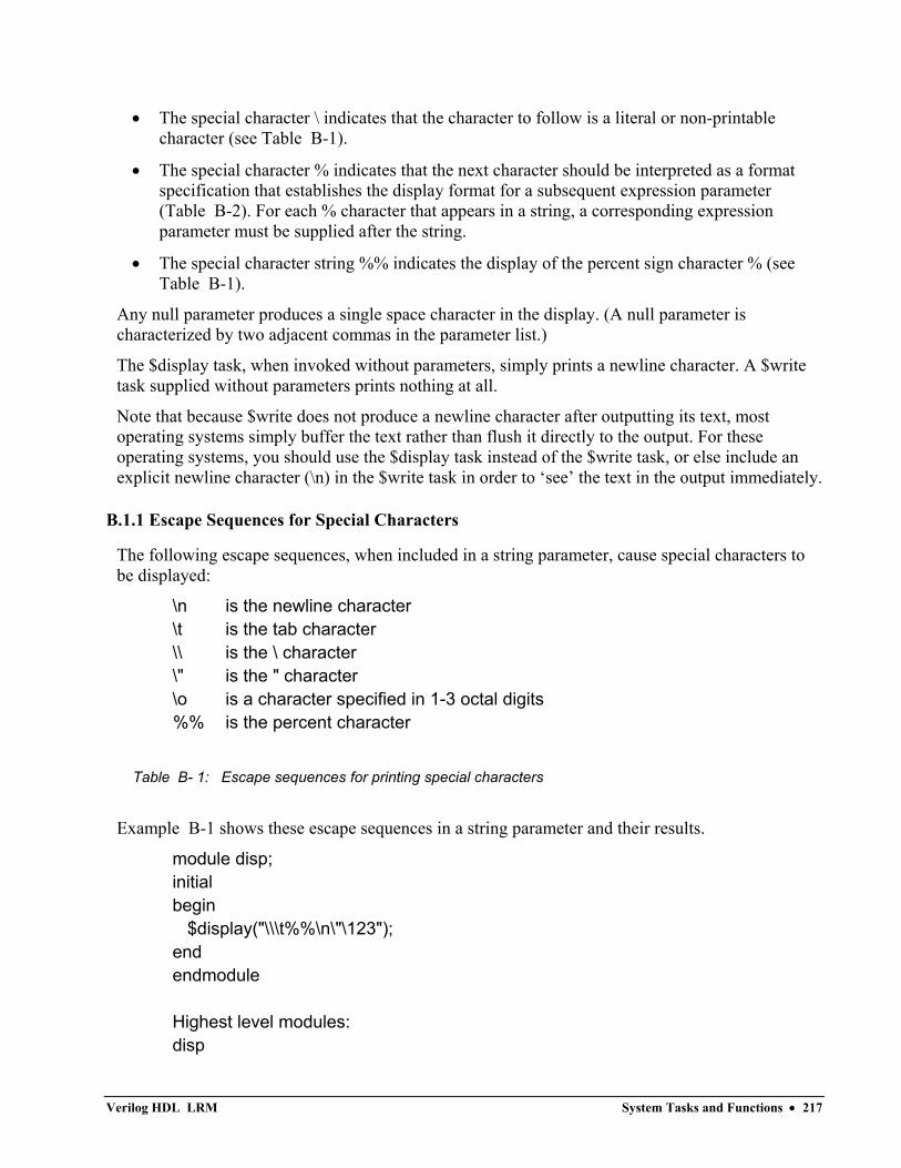
• The special character \ indicates that the character to follow is a literal or non-printable character (see Table B-1).
• The special character % indicates that the next character should be interpreted as a format specification that establishes the display format for a subsequent expression parameter (Table B-2). For each % character that appears in a string, a corresponding expression parameter must be supplied after the string.
• The special character string %% indicates the display of the percent sign character % (see Table B-1).
Any null parameter produces a single space character in the display. (A null parameter is characterized by two adjacent commas in the parameter list.)
The $display task, when invoked without parameters, simply prints a newline character. A $write task supplied without parameters prints nothing at all.
Note that because $write does not produce a newline character after outputting its text, most operating systems simply buffer the text rather than flush it directly to the output. For these operating systems, you should use the $display task instead of the $write task, or else include an explicit newline character (\n) in the $write task in order to ‘see’ the text in the output immediately.
B.1.1 Escape Sequences for Special Characters
The following escape sequences, when included in a string parameter, cause special characters to be displayed:
\n is the newline character \t is the tab character \\ is the \ character \" is the " character \o is a character specified in 1-3 octal digits %% is the percent character
Table B- 1: Escape sequences for printing special characters
Example B-1 shows these escape sequences in a string parameter and their results.
module disp; initial begin $display("\\\t%%\n\"\123"); end endmodule Highest level modules: disp
Verilog HDL LRM System Tasks and Functions • 217
\ % "S
Example B- 1: Using escape sequences
B.1.2 Format Specifications
Table B-2 shows the escape sequences used for format specifications. Each escape sequence, when included in a string parameter, specifies the display format for a subsequent expression. For each % character (except %m) that appears in a string, a corresponding expression must follow the string in the parameter list. The value of the expression replaces the format specification when the string is displayed.
Any expression parameter that has no corresponding format specification is displayed using the default decimal format.
%h or %H display in hexadecimal format %d or %D display in decimal format %o or %O display in octal format %b or %B display in binary format %c or %C display in ASCII character format %v or %V display net signal strength %m or %M display hierarchical name %s or %S display as a string %t or %T display in current time format
Table B- 2: Escape sequences for format specifications
Example B-2 shows how escape sequences are used to provide format specifications.
module disp; reg [31:0] rval; pulldown (pd); initial begin rval = 101; $display("rval = %h hex %d decimal",rval,rval); $display("rval = %o octal %b binary",rval,rval); $display("rval has %c ascii character value",rval); $display("pd strength value is %v",pd); $display("current scope is %m"); $display("%s is ascii value for 101",101); $display("simulation time is %t", $time); end
Verilog HDL LRM System Tasks and Functions • 218
endmodule Highest level modules: disp
rval = 00000065 hex 101 decimal rval = 00000000145 octal 00000000000000000000000001100101 binary rval has e ascii character value pd strength value is StX current scope is disp e is ascii value for 101 simulation time is 0
Example B- 2: Format specifications
The format specifications in Table B-3 are used with real numbers and have the full formatting capabilities available in the C language. For example, the format specification %10.3g specifies a minimum field width of 10 with 3 fractional digits.
%e or %E display `real' in an exponential format %f or %F display `real' in a decimal format %g or %G display `real' in exponential or decimal format, whichever format
results in the shorter printed output
Table B- 3: Format specifications for real numbers
The net signal strength, hierarchical name, and string format specifications are described in sections B.1.5 Strength Format through B.1.7 String Format. The %t format specification works with the $timeformat system task to specify a uniform time unit, time precision, and format for reporting timing information from various modules that use different time units and precisions. The $timeformat task and %t format specification are described in Section B.4 Timescale System Functions Timescale System Functions.
B.1.3 Size of Displayed Data
For expression parameters, the values written to the output file (or terminal) are usually sized automatically. Verilog reserves just enough characters to hold the largest possible value that can be returned by the expression, given the expression’s bit length and specified display format.
For instance, the result of a 12-bit expression would be allocated three characters when displayed in hexadecimal format and four characters when displayed in decimal format, since the expression’s largest possible value is FFF (hexadecimal) and 4095 (decimal).
When displaying decimal values, leading zeros are suppressed and replaced by spaces. In other radices, leading zeros are always displayed.
You can override the automatic sizing of displayed data by inserting a zero between the % character and the letter that indicates the radix, as shown below:
Verilog HDL LRM System Tasks and Functions • 219
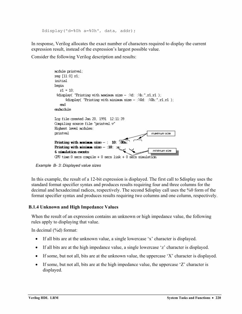
$display("d=%0h a=%0h", data, addr);
In response, Verilog allocates the exact number of characters required to display the current expression result, instead of the expression’s largest possible value. Consider the following Verilog description and results:
Example B- 3: Displayed value sizes
In this example, the result of a 12-bit expression is displayed. The first call to $display uses the standard format specifier syntax and produces results requiring four and three columns for the decimal and hexadecimal radices, respectively. The second $display call uses the %0 form of the format specifier syntax and produces results requiring two columns and one column, respectively.
B.1.4 Unknown and High Impedance Values
When the result of an expression contains an unknown or high impedance value, the following rules apply to displaying that value.
In decimal (%d) format:
• If all bits are at the unknown value, a single lowercase ‘x’ character is displayed.
• If all bits are at the high impedance value, a single lowercase ‘z’ character is displayed.
• If some, but not all, bits are at the unknown value, the uppercase ‘X’ character is displayed.
• If some, but not all, bits are at the high impedance value, the uppercase ‘Z’ character is displayed.
Verilog HDL LRM System Tasks and Functions • 220
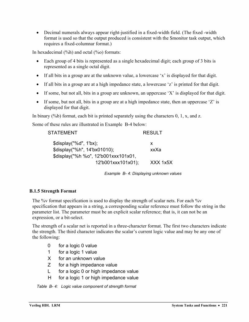
• Decimal numerals always appear right-justified in a fixed-width field. (The fixed -width format is used so that the output produced is consistent with the $monitor task output, which requires a fixed-columnar format.)
In hexadecimal (%h) and octal (%o) formats:
• Each group of 4 bits is represented as a single hexadecimal digit; each group of 3 bits is represented as a single octal digit.
• If all bits in a group are at the unknown value, a lowercase ‘x’ is displayed for that digit.
• If all bits in a group are at a high impedance state, a lowercase ‘z’ is printed for that digit.
• If some, but not all, bits in a group are unknown, an uppercase ‘X’ is displayed for that digit.
• If some, but not all, bits in a group are at a high impedance state, then an uppercase ‘Z’ is displayed for that digit.
In binary (%b) format, each bit is printed separately using the characters 0, 1, x, and z.
Some of these rules are illustrated in Example B-4 below:
STATEMENT RESULT
$display("%d", 1'bx); x $display("%h", 14'bx01010); xxXa $display("%h %o", 12'b001xxx101x01, 12'b001xxx101x01); XXX 1x5X
Example B- 4: Displaying unknown values
B.1.5 Strength Format
The %v format specification is used to display the strength of scalar nets. For each %v specification that appears in a string, a corresponding scalar reference must follow the string in the parameter list. The parameter must be an explicit scalar reference; that is, it can not be an expression, or a bit-select.
The strength of a scalar net is reported in a three-character format. The first two characters indicate the strength. The third character indicates the scalar’s current logic value and may be any one of the following:
0 for a logic 0 value 1 for a logic 1 value X for an unknown value Z for a high impedance value L for a logic 0 or high impedance value H for a logic 1 or high impedance value
Table B- 4: Logic value component of strength format
Verilog HDL LRM System Tasks and Functions • 221
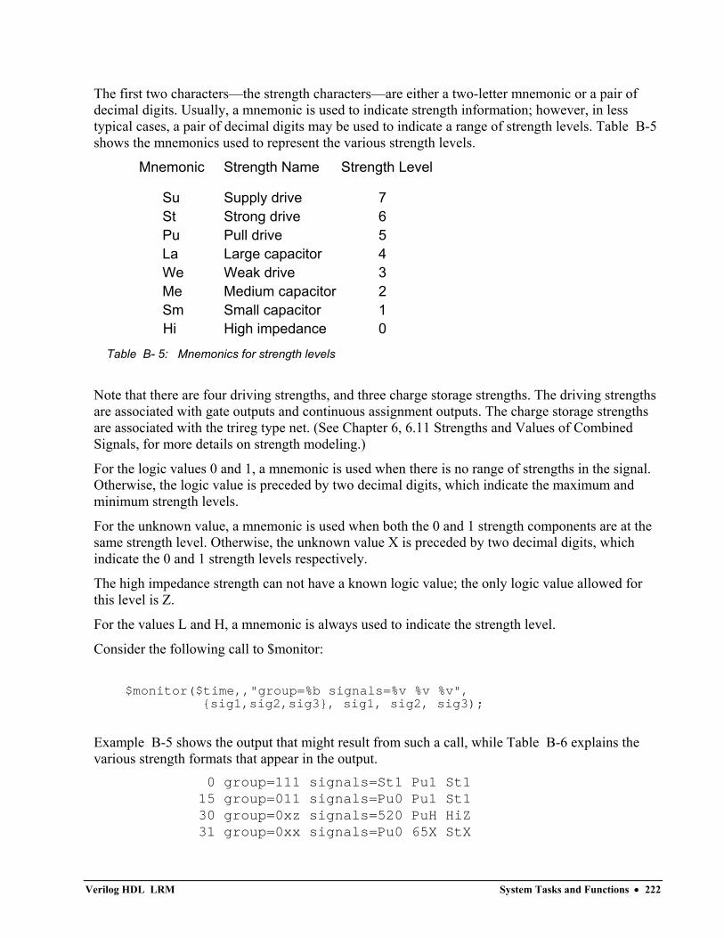
The first two characters—the strength characters—are either a two-letter mnemonic or a pair of decimal digits. Usually, a mnemonic is used to indicate strength information; however, in less typical cases, a pair of decimal digits may be used to indicate a range of strength levels. Table B-5 shows the mnemonics used to represent the various strength levels.
Mnemonic Strength Name Strength Level
Su Supply drive 7 St Strong drive 6 Pu Pull drive 5 La Large capacitor 4 We Weak drive 3 Me Medium capacitor 2 Sm Small capacitor 1 Hi High impedance 0
Table B- 5: Mnemonics for strength levels
Note that there are four driving strengths, and three charge storage strengths. The driving strengths are associated with gate outputs and continuous assignment outputs. The charge storage strengths are associated with the trireg type net. (See Chapter 6, 6.11 Strengths and Values of Combined Signals, for more details on strength modeling.)
For the logic values 0 and 1, a mnemonic is used when there is no range of strengths in the signal. Otherwise, the logic value is preceded by two decimal digits, which indicate the maximum and minimum strength levels.
For the unknown value, a mnemonic is used when both the 0 and 1 strength components are at the same strength level. Otherwise, the unknown value X is preceded by two decimal digits, which indicate the 0 and 1 strength levels respectively.
The high impedance strength can not have a known logic value; the only logic value allowed for this level is Z.
For the values L and H, a mnemonic is always used to indicate the strength level.
Consider the following call to $monitor:
$monitor($time,,"group=%b signals=%v %v %v", {sig1,sig2,sig3}, sig1, sig2, sig3);
Example B-5 shows the output that might result from such a call, while Table B-6 explains the various strength formats that appear in the output.
0 group=111 signals=St1 Pu1 St1 15 group=011 signals=Pu0 Pu1 St1 30 group=0xz signals=520 PuH HiZ 31 group=0xx signals=Pu0 65X StX
Verilog HDL LRM System Tasks and Functions • 222
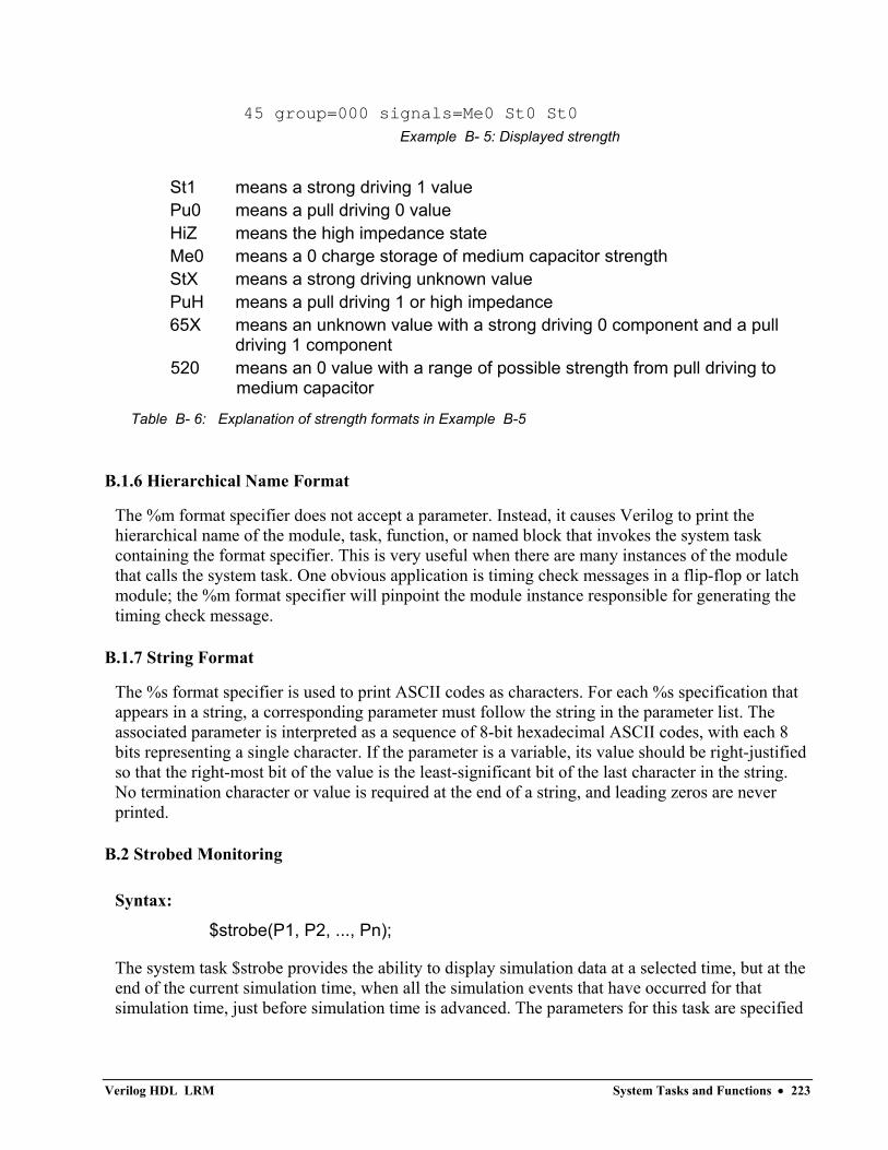
45 group=000 signals=Me0 St0 St0
Example B- 5: Displayed strength
St1 means a strong driving 1 value Pu0 means a pull driving 0 value HiZ means the high impedance state Me0 means a 0 charge storage of medium capacitor strength StX means a strong driving unknown value PuH means a pull driving 1 or high impedance 65X means an unknown value with a strong driving 0 component and a pull
driving 1 component 520 means an 0 value with a range of possible strength from pull driving to
medium capacitor
Table B- 6: Explanation of strength formats in Example B-5
B.1.6 Hierarchical Name Format
The %m format specifier does not accept a parameter. Instead, it causes Verilog to print the hierarchical name of the module, task, function, or named block that invokes the system task containing the format specifier. This is very useful when there are many instances of the module that calls the system task. One obvious application is timing check messages in a flip-flop or latch module; the %m format specifier will pinpoint the module instance responsible for generating the timing check message.
B.1.7 String Format
The %s format specifier is used to print ASCII codes as characters. For each %s specification that appears in a string, a corresponding parameter must follow the string in the parameter list. The associated parameter is interpreted as a sequence of 8-bit hexadecimal ASCII codes, with each 8 bits representing a single character. If the parameter is a variable, its value should be right-justified so that the right-most bit of the value is the least-significant bit of the last character in the string. No termination character or value is required at the end of a string, and leading zeros are never printed.
B.2 Strobed Monitoring
Syntax:
$strobe(P1, P2, ..., Pn);
The system task $strobe provides the ability to display simulation data at a selected time, but at the end of the current simulation time, when all the simulation events that have occurred for that simulation time, just before simulation time is advanced. The parameters for this task are specified
Verilog HDL LRM System Tasks and Functions • 223
in exactly the same manner as for the $display system task—including the use of escape sequences for special characters and format specifications (see Section B.1 The Display and Write Tasks).
The following example shows how the $strobe system task is used:
forever @(negedge clock) $strobe ("At time %d, data is %h",$time,data);
In this example, $strobe will write the time and data information to the standard output and the log file at each negative edge of the clock. The action will occur just before simulation time is advanced, after all other events at that time have occurred, so that the data written is sure to be the correct data for that simulation time.
The strobe tasks produce output when they are executed and there is no on/off control necessary.
B.3 Continuous Monitoring
Syntax:
$monitor(P1, P2, ..., Pn); $monitor; $monitoron; $monitoroff;
The $monitor task provides the ability to monitor and display the values of any variables or expressions specified as parameters to the task. The parameters for this task are specified in exactly the same manner as for the $display system task—including the use of escape sequences for special characters and format specifications (see Section B.1 The Display and Write Tasks).
When you invoke a $monitor task with one or more parameters, the simulator sets up a mechanism whereby each time a variable or an expression in the parameter list changes value–with the exception of the $time, $stime or $realtime system functions–the entire parameter list is displayed at the end of the time step as if reported by the $display task. If two or more parameters change value at the same time, however, only one display is produced that shows the new values.
Note that only one $monitor display list can be active at any one time; however, you can issue a new $monitor task with a new display list any number of times during simulation.
The $monitoron and $monitoroff tasks control a monitor flag that enables and disables the monitoring, so that you can easily control when monitoring should occur. Use $monitoroff to turn off the flag and disable monitoring. Use $monitoron to turn on the flag so that monitoring is enabled and the most recent call to $monitor can resume its display. A call to $monitoron always produces a display immediately after it is invoked, regardless of whether a value change has taken place; this is used to establish the initial values at the beginning of a monitoring session. By default, the monitor flag is turned on at the beginning of simulation.
Verilog HDL LRM System Tasks and Functions • 224
For $monitor tasks issued interactively, there is an alternative method for controlling when monitoring should occur. The method involves using the disable command to turn off a $monitor command and then re-executing the command to turn monitoring back on. Example B-6 illustrates this technique.
C3> $monitor($time,,"rxd=%btxd=%b",rxd,txd); C4> #100 $stop;. 0 rxd=1 txd=1 20 rxd=0 txd=1 60 rxd=0 txd=0 80 rxd=0 txd=1 C4: $stop at simulation time 100 C5> -3
Example B- 6: Using $monitor interactively
In this example, monitoring is allowed to occur for the first 100 time units of the simulation before the disable command is issued at C5. The disable command is issued by identifying the command number of the interactive command you wish to disable and typing a minus sign before it. Here, by typing -3, we disable command 3, which invokes the $monitor task. Later in the simulation, by typing a 3 at the interactive command prompt, we can re-execute command 3 to resume monitoring.
B.4 Timescale System Functions
The following are timescale system functions:
• $time
• $realtime
The $time and $realtime system functions allow you to access the current simulation time.
B.4.1 The $time System Function
The $time system function returns an integer that is a 64-bit time, scaled to the timescale unit of the module that invoked it.
Here is an example:
`timescale 10 ns / 1 ns module test; reg set; parameter p = 1.55; initial begin $monitor($time,,"set=",set);
Verilog HDL LRM System Tasks and Functions • 225
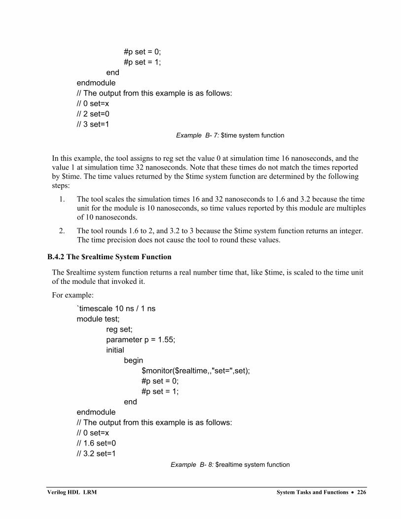
#p set = 0; #p set = 1; end endmodule // The output from this example is as follows: // 0 set=x // 2 set=0 // 3 set=1
Example B- 7: $time system function
In this example, the tool assigns to reg set the value 0 at simulation time 16 nanoseconds, and the value 1 at simulation time 32 nanoseconds. Note that these times do not match the times reported by $time. The time values returned by the $time system function are determined by the following steps:
1. The tool scales the simulation times 16 and 32 nanoseconds to 1.6 and 3.2 because the time unit for the module is 10 nanoseconds, so time values reported by this module are multiples of 10 nanoseconds.
2. The tool rounds 1.6 to 2, and 3.2 to 3 because the $time system function returns an integer. The time precision does not cause the tool to round these values.
B.4.2 The $realtime System Function
The $realtime system function returns a real number time that, like $time, is scaled to the time unit of the module that invoked it.
For example:
`timescale 10 ns / 1 ns module test; reg set; parameter p = 1.55; initial begin $monitor($realtime,,"set=",set); #p set = 0; #p set = 1; end endmodule // The output from this example is as follows: // 0 set=x // 1.6 set=0 // 3.2 set=1
Example B- 8: $realtime system function
Verilog HDL LRM System Tasks and Functions • 226
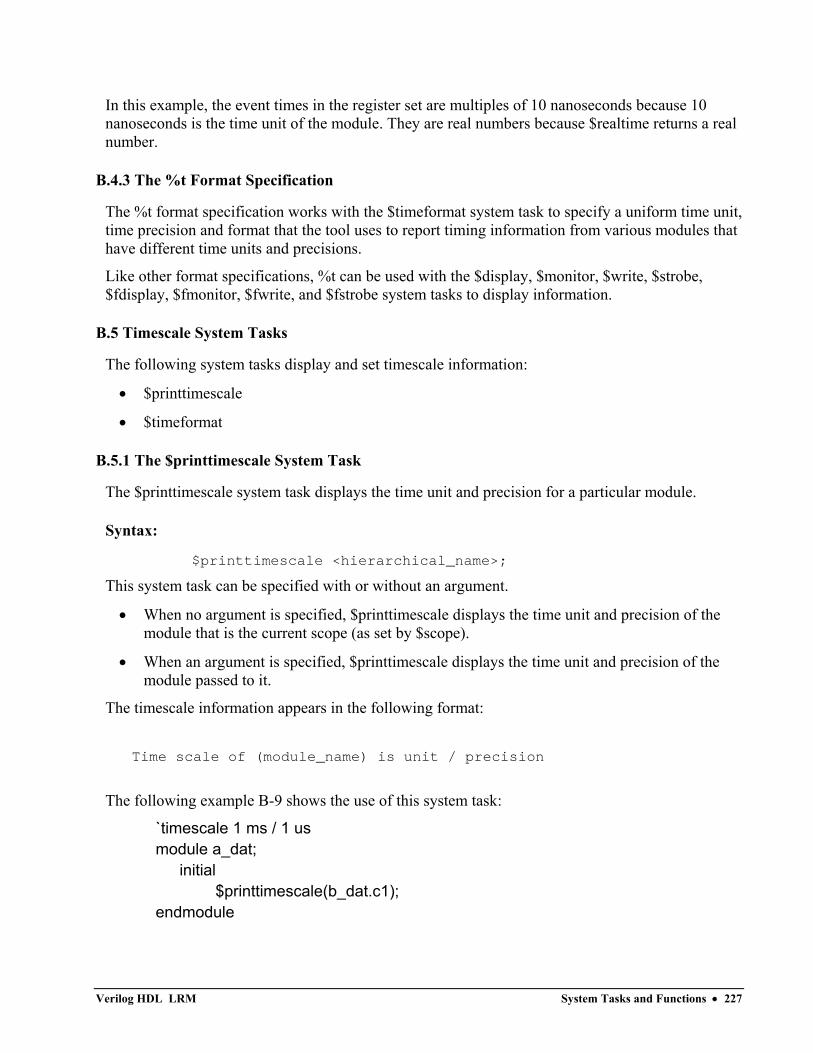
In this example, the event times in the register set are multiples of 10 nanoseconds because 10 nanoseconds is the time unit of the module. They are real numbers because $realtime returns a real number.
B.4.3 The %t Format Specification
The %t format specification works with the $timeformat system task to specify a uniform time unit, time precision and format that the tool uses to report timing information from various modules that have different time units and precisions.
Like other format specifications, %t can be used with the $display, $monitor, $write, $strobe, $fdisplay, $fmonitor, $fwrite, and $fstrobe system tasks to display information.
B.5 Timescale System Tasks
The following system tasks display and set timescale information:
• $printtimescale
• $timeformat
B.5.1 The $printtimescale System Task
The $printtimescale system task displays the time unit and precision for a particular module.
Syntax:
$printtimescale <hierarchical_name>;
This system task can be specified with or without an argument.
• When no argument is specified, $printtimescale displays the time unit and precision of the module that is the current scope (as set by $scope).
• When an argument is specified, $printtimescale displays the time unit and precision of the module passed to it.
The timescale information appears in the following format:
Time scale of (module_name) is unit / precision
The following example B-9 shows the use of this system task:
`timescale 1 ms / 1 us module a_dat; initial $printtimescale(b_dat.c1); endmodule
Verilog HDL LRM System Tasks and Functions • 227
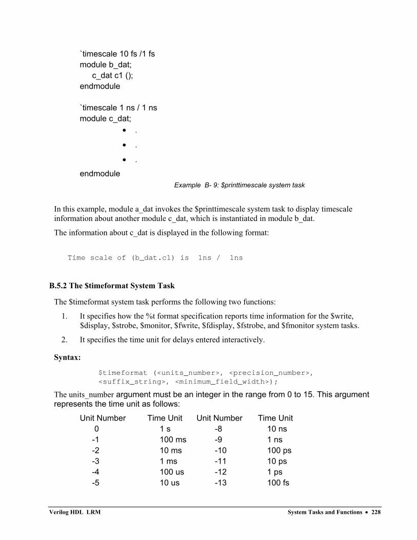
`timescale 10 fs /1 fs module b_dat; c_dat c1 (); endmodule `timescale 1 ns / 1 ns module c_dat;
• .
• .
• .
endmodule Example B- 9: $printtimescale system task
In this example, module a_dat invokes the $printtimescale system task to display timescale information about another module c_dat, which is instantiated in module b_dat.
The information about c_dat is displayed in the following format:
Time scale of (b_dat.c1) is 1ns / 1ns
B.5.2 The $timeformat System Task
The $timeformat system task performs the following two functions:
1. It specifies how the %t format specification reports time information for the $write, $display, $strobe, $monitor, $fwrite, $fdisplay, $fstrobe, and $fmonitor system tasks.
2. It specifies the time unit for delays entered interactively.
Syntax:
$timeformat (<units_number>, <precision_number>, <suffix_string>, <minimum_field_width>);
The units_number argument must be an integer in the range from 0 to 15. This argument represents the time unit as follows:
Unit Number Time Unit Unit Number Time Unit 0 1 s -8 10 ns -1 100 ms -9 1 ns -2 10 ms -10 100 ps -3 1 ms -11 10 ps -4 100 us -12 1 ps -5 10 us -13 100 fs
Verilog HDL LRM System Tasks and Functions • 228
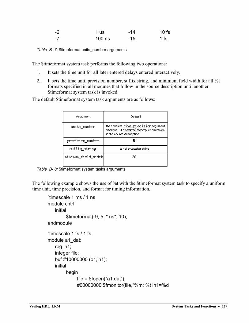
-6 1 us -14 10 fs -7 100 ns -15 1 fs
Table B- 7: $timeformat units_number arguments
The $timeformat system task performs the following two operations:
1. It sets the time unit for all later entered delays entered interactively.
2. It sets the time unit, precision number, suffix string, and minimum field width for all %t formats specified in all modules that follow in the source description until another $timeformat system task is invoked.
The default $timeformat system task arguments are as follows:
Table B- 8: $timeformat system tasks arguments
The following example shows the use of %t with the $timeformat system task to specify a uniform time unit, time precision, and format for timing information.
`timescale 1 ms / 1 ns module cntrl; initial $timeformat(-9, 5, " ns", 10); endmodule
`timescale 1 fs / 1 fs module a1_dat; reg in1; integer file; buf #10000000 (o1,in1); initial begin file = $fopen("a1.dat"); #00000000 $fmonitor(file,"%m: %t in1=%d
Verilog HDL LRM System Tasks and Functions • 229
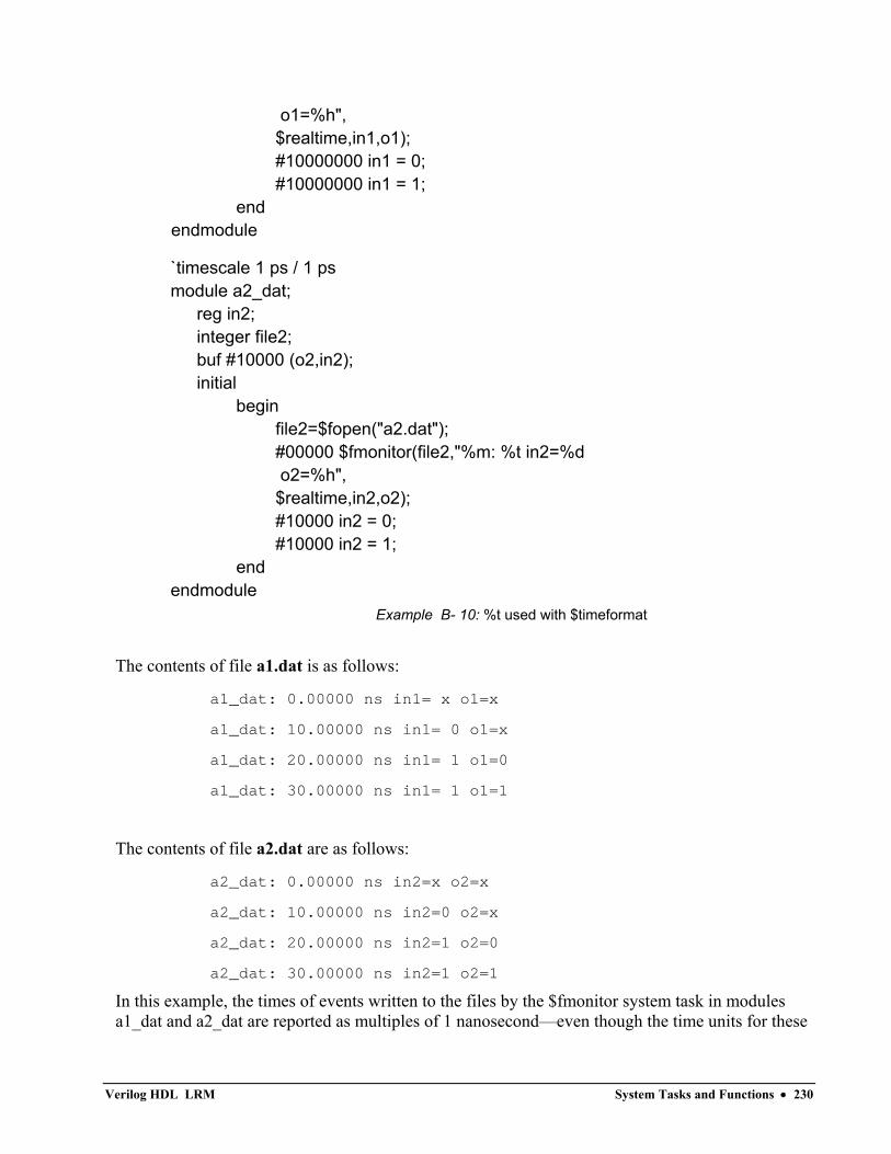
o1=%h", $realtime,in1,o1); #10000000 in1 = 0; #10000000 in1 = 1; end endmodule
`timescale 1 ps / 1 ps module a2_dat; reg in2; integer file2; buf #10000 (o2,in2); initial begin file2=$fopen("a2.dat"); #00000 $fmonitor(file2,"%m: %t in2=%d o2=%h", $realtime,in2,o2); #10000 in2 = 0; #10000 in2 = 1; end endmodule
Example B- 10: %t used with $timeformat
The contents of file a1.dat is as follows:
a1_dat: 0.00000 ns in1= x o1=x
a1_dat: 10.00000 ns in1= 0 o1=x
a1_dat: 20.00000 ns in1= 1 o1=0
a1_dat: 30.00000 ns in1= 1 o1=1
The contents of file a2.dat are as follows:
a2_dat: 0.00000 ns in2=x o2=x
a2_dat: 10.00000 ns in2=0 o2=x
a2_dat: 20.00000 ns in2=1 o2=0
a2_dat: 30.00000 ns in2=1 o2=1
In this example, the times of events written to the files by the $fmonitor system task in modules a1_dat and a2_dat are reported as multiples of 1 nanosecond—even though the time units for these
Verilog HDL LRM System Tasks and Functions • 230
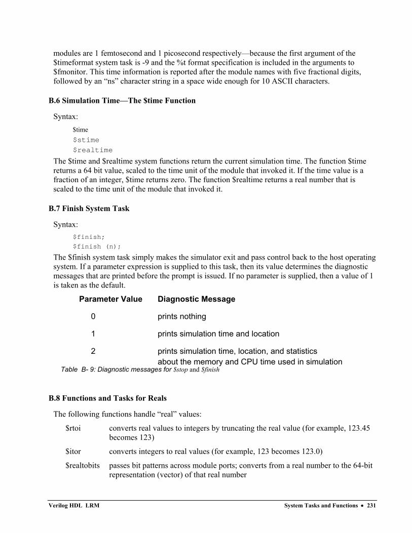
modules are 1 femtosecond and 1 picosecond respectively—because the first argument of the $timeformat system task is -9 and the %t format specification is included in the arguments to $fmonitor. This time information is reported after the module names with five fractional digits, followed by an “ns” character string in a space wide enough for 10 ASCII characters.
B.6 Simulation Time—The $time Function
Syntax: $time $stime
$realtime
The $time and $realtime system functions return the current simulation time. The function $time returns a 64 bit value, scaled to the time unit of the module that invoked it. If the time value is a fraction of an integer, $time returns zero. The function $realtime returns a real number that is scaled to the time unit of the module that invoked it.
B.7 Finish System Task
Syntax: $finish;
$finish (n);
The $finish system task simply makes the simulator exit and pass control back to the host operating system. If a parameter expression is supplied to this task, then its value determines the diagnostic messages that are printed before the prompt is issued. If no parameter is supplied, then a value of 1 is taken as the default.
Parameter Value Diagnostic Message
0 prints nothing
1 prints simulation time and location
2 prints simulation time, location, and statistics about the memory and CPU time used in simulation
Table B- 9: Diagnostic messages for $stop and $finish
B.8 Functions and Tasks for Reals
The following functions handle “real” values:
$rtoi converts real values to integers by truncating the real value (for example, 123.45 becomes 123)
$itor converts integers to real values (for example, 123 becomes 123.0)
$realtobits passes bit patterns across module ports; converts from a real number to the 64-bit representation (vector) of that real number
Verilog HDL LRM System Tasks and Functions • 231
$bitstoreal is the reverse of $realtobits; converts from the bit pattern to a real number
Example B-11 shows how the $realtobits and $bitstoreal functions are used in port connections.
module driver (net_r); output net_r; real r; wire [64:1] net_r = $realtobits(r); endmodule
module receiver (net_r); input net_r; wire [64:1] net_r; real r; initial assign r =$bitstoreal(net_r); endmodule
Example B- 11: Using $realtobits and $bitstoreal
B.9 Timing Checks
You may invoke timing checks in specify blocks to verify the timing performance of your design by making sure critical events occur within given time limits.
Timing checks perform the following steps:
1. Determine the elapsed time between two events.
2. Compare the elapsed time to a specified limit. 3. If the elapsed time does not fall within the specified time window, report a timing violation.
Here is a sample timing check message from SILOS III:
"pdmf2.vo", 10164: Timing violation at 2548 in top.pdmf2_inst.MUX_SEL_SYNC1
$setup(D:2545, (posedge CLK)&&&legal:2548, "3 < 13");
The $setup system task is in file pdmf2.vo at line 10164. The setup violation occurred at time=2548 in instance top.pdmf2_inst.MUX_SEL_SYNC1. The "D" net changed at time=2545, and the expression (posedge CLK)&&&legal changed at time=2548. This delta of 3 is less than the specified setup time of 13.
Here is a list of system tasks available for performing timing checks:
$setup( data_event, reference_event, limit , notifier ); $hold( reference_event, data_event, limit , notifier ); $width( reference_event, limit , threshold, notifier ); $period(reference_event, limit , notifier ); $skew( reference_event, data_event, limit , notifier ); $recovery( reference_event, data_event, limit , notifier ); $setuphold( reference_event, data_event, setup_limit, hold_limit, notifier;
Verilog HDL LRM System Tasks and Functions • 232
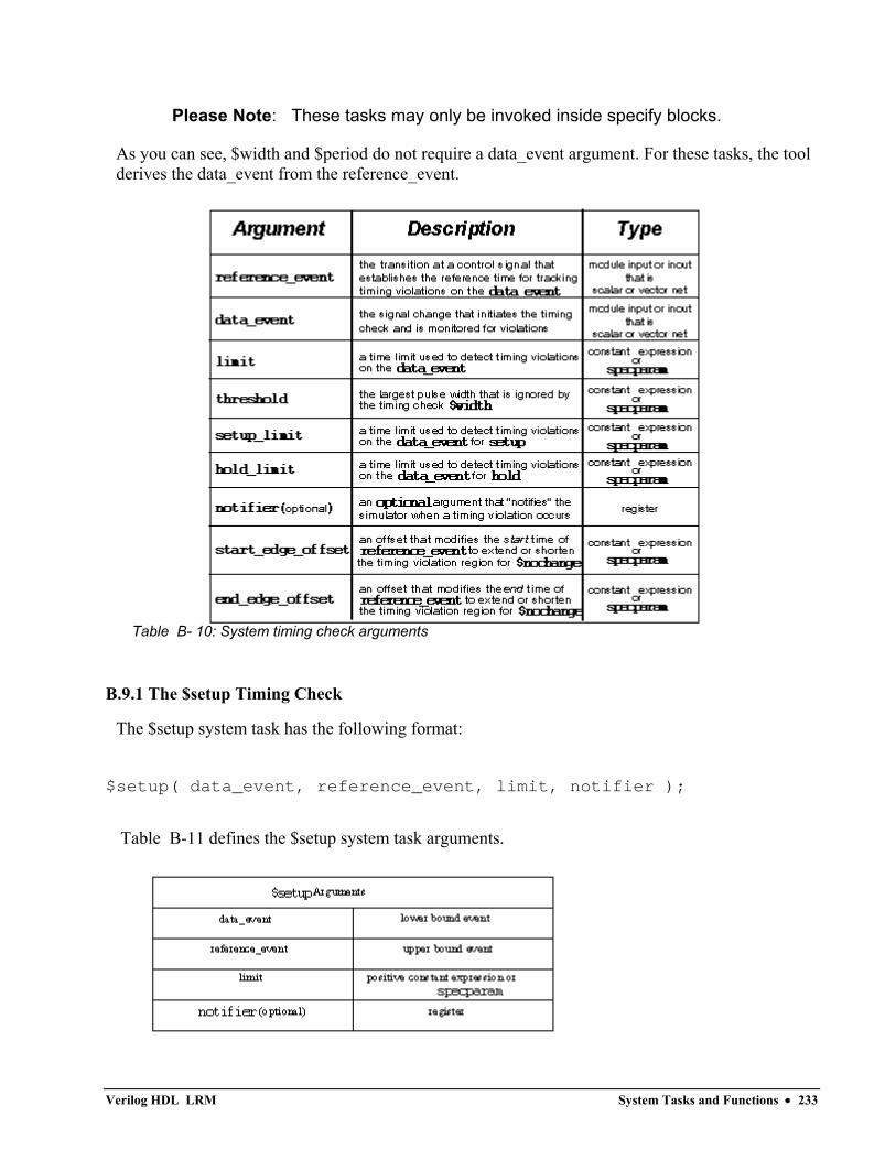
Please Note: These tasks may only be invoked inside specify blocks.
As you can see, $width and $period do not require a data_event argument. For these tasks, the tool derives the data_event from the reference_event.
Table B- 10: System timing check arguments
B.9.1 The $setup Timing Check
The $setup system task has the following format:
$setup( data_event, reference_event, limit, notifier );
Table B-11 defines the $setup system task arguments.
Verilog HDL LRM System Tasks and Functions • 233
Table B- 11: $setup arguments
The $setup timing check reports a timing violation in the following case:
(time of reference_event)-(time of data_event) < limit
If the reference_event and data_event occur simultaneously, $setup performs the timing check before it records the new data_event value, therefore no violation occurs.
B.9.2 The $hold Timing Check
The $hold system task has the following format:
$hold(reference_event,data_event,limit,notifier);
Table B-12 defines the $hold system task arguments.
Table B- 12: Arguments of $hold
$hold reports a violation in the following case:
(time of data_event) - (time of reference_event) < limit
$hold always records the new reference_event time before it performs the timing check. Therefore, if simultaneous events occur, there will be a violation.
B.9.3 The $width Timing Check
The $width system task has the following format:
$width(reference_event,limit,threshold,notifier);
Verilog HDL LRM System Tasks and Functions • 234
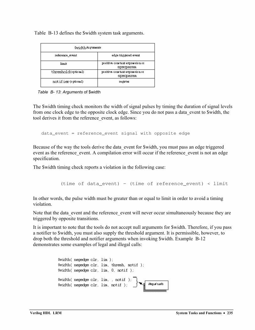
Table B-13 defines the $width system task arguments.
Table B- 13: Arguments of $width
The $width timing check monitors the width of signal pulses by timing the duration of signal levels from one clock edge to the opposite clock edge. Since you do not pass a data_event to $width, the tool derives it from the reference_event, as follows:
data_event = reference_event signal with opposite edge
Because of the way the tools derive the data_event for $width, you must pass an edge triggered event as the reference_event. A compilation error will occur if the reference_event is not an edge specification.
The $width timing check reports a violation in the following case:
(time of data_event) - (time of reference_event) < limit
In other words, the pulse width must be greater than or equal to limit in order to avoid a timing violation.
Note that the data_event and the reference_event will never occur simultaneously because they are triggered by opposite transitions.
It is important to note that the tools do not accept null arguments for $width. Therefore, if you pass a notifier to $width, you must also supply the threshold argument. It is permissible, however, to drop both the threshold and notifier arguments when invoking $width. Example B-12 demonstrates some examples of legal and illegal calls:
Verilog HDL LRM System Tasks and Functions • 235
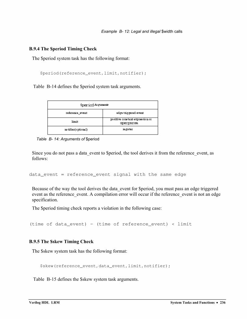
Example B- 12: Legal and illegal $width calls
B.9.4 The $period Timing Check
The $period system task has the following format:
$period(reference_event,limit,notifier);
Table B-14 defines the $period system task arguments.
Table B- 14: Arguments of $period
Since you do not pass a data_event to $period, the tool derives it from the reference_event, as follows:
data_event = reference_event signal with the same edge
Because of the way the tool derives the data_event for $period, you must pass an edge triggered event as the reference_event. A compilation error will occur if the reference_event is not an edge specification.
The $period timing check reports a violation in the following case:
(time of data_event) - (time of reference_event) < limit
B.9.5 The $skew Timing Check
The $skew system task has the following format:
$skew(reference_event,data_event,limit,notifier);
Table B-15 defines the $skew system task arguments.
Verilog HDL LRM System Tasks and Functions • 236
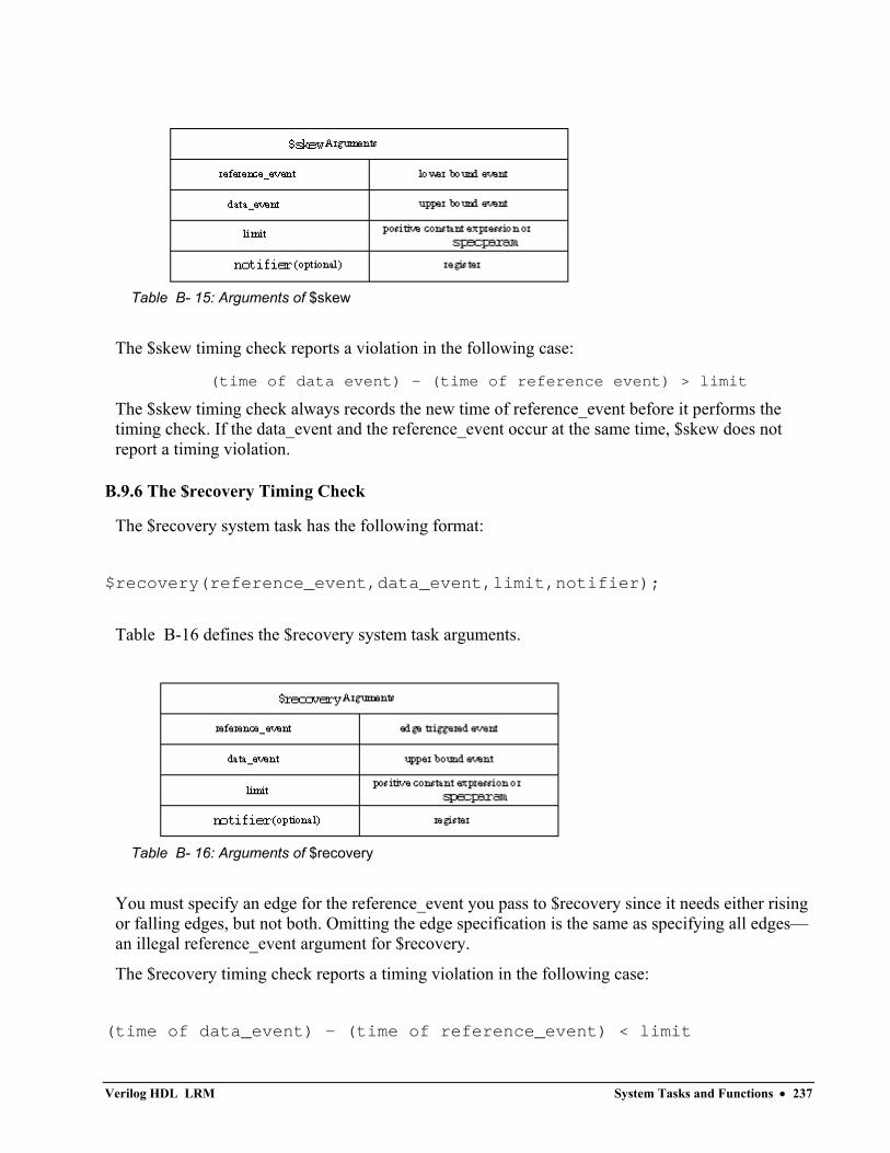
Table B- 15: Arguments of $skew
The $skew timing check reports a violation in the following case:
(time of data event) - (time of reference event) > limit
The $skew timing check always records the new time of reference_event before it performs the timing check. If the data_event and the reference_event occur at the same time, $skew does not report a timing violation.
B.9.6 The $recovery Timing Check
The $recovery system task has the following format:
$recovery(reference_event,data_event,limit,notifier);
Table B-16 defines the $recovery system task arguments.
Table B- 16: Arguments of $recovery
You must specify an edge for the reference_event you pass to $recovery since it needs either rising or falling edges, but not both. Omitting the edge specification is the same as specifying all edges—an illegal reference_event argument for $recovery.
The $recovery timing check reports a timing violation in the following case:
(time of data_event) - (time of reference_event) < limit
Verilog HDL LRM System Tasks and Functions • 237
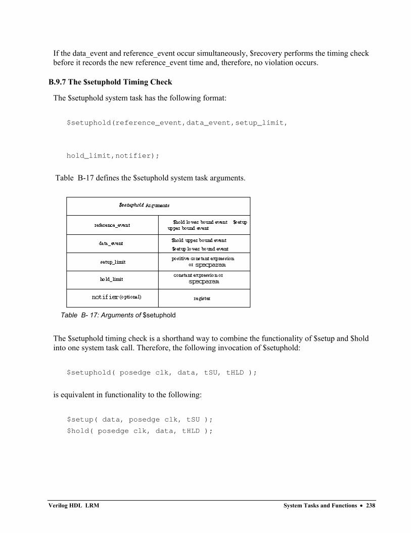
If the data_event and reference_event occur simultaneously, $recovery performs the timing check before it records the new reference_event time and, therefore, no violation occurs.
B.9.7 The $setuphold Timing Check
The $setuphold system task has the following format:
$setuphold(reference_event,data_event,setup_limit,
hold_limit,notifier);
Table B-17 defines the $setuphold system task arguments.
Table B- 17: Arguments of $setuphold
The $setuphold timing check is a shorthand way to combine the functionality of $setup and $hold into one system task call. Therefore, the following invocation of $setuphold:
$setuphold( posedge clk, data, tSU, tHLD );
is equivalent in functionality to the following:
$setup( data, posedge clk, tSU );
$hold( posedge clk, data, tHLD );
Verilog HDL LRM System Tasks and Functions • 238
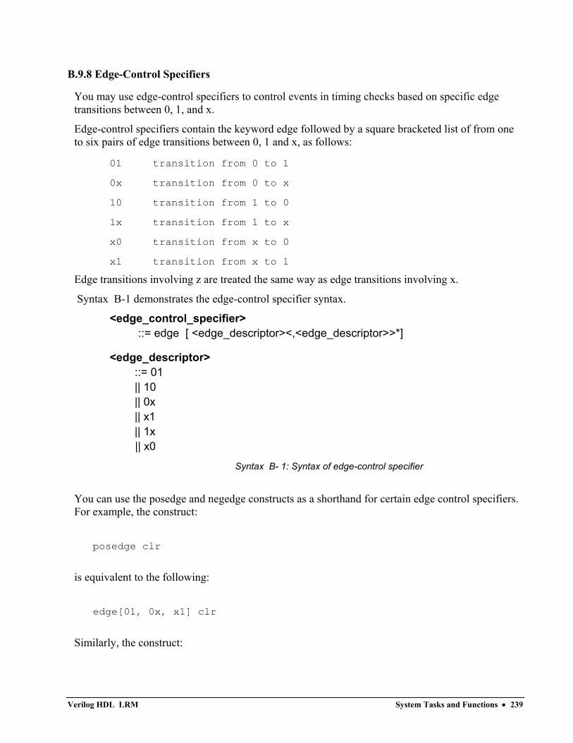
B.9.8 Edge-Control Specifiers
You may use edge-control specifiers to control events in timing checks based on specific edge transitions between 0, 1, and x.
Edge-control specifiers contain the keyword edge followed by a square bracketed list of from one to six pairs of edge transitions between 0, 1 and x, as follows:
01 transition from 0 to 1
0x transition from 0 to x
10 transition from 1 to 0
1x transition from 1 to x
x0 transition from x to 0
x1 transition from x to 1
Edge transitions involving z are treated the same way as edge transitions involving x.
Syntax B-1 demonstrates the edge-control specifier syntax.
<edge_control_specifier> ::= edge [ <edge_descriptor><,<edge_descriptor>>*]
<edge_descriptor> ::= 01 || 10 || 0x || x1 || 1x || x0
Syntax B- 1: Syntax of edge-control specifier
You can use the posedge and negedge constructs as a shorthand for certain edge control specifiers. For example, the construct:
posedge clr
is equivalent to the following:
edge[01, 0x, x1] clr
Similarly, the construct:
Verilog HDL LRM System Tasks and Functions • 239
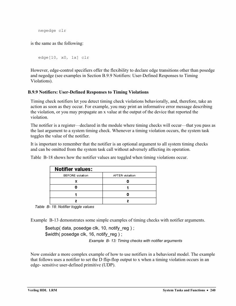
negedge clr
is the same as the following:
edge[10, x0, 1x] clr
However, edge-control specifiers offer the flexibility to declare edge transitions other than posedge and negedge (see examples in Section B.9.9 Notifiers: User-Defined Responses to Timing Violations).
B.9.9 Notifiers: User-Defined Responses to Timing Violations
Timing check notifiers let you detect timing check violations behaviorally, and, therefore, take an action as soon as they occur. For example, you may print an informative error message describing the violation, or you may propagate an x value at the output of the device that reported the violation.
The notifier is a register—declared in the module where timing checks will occur—that you pass as the last argument to a system timing check. Whenever a timing violation occurs, the system task toggles the value of the notifier.
It is important to remember that the notifier is an optional argument to all system timing checks and can be omitted from the system task call without adversely affecting its operation.
Table B-18 shows how the notifier values are toggled when timing violations occur.
Table B- 18: Notifier toggle values
Example B-13 demonstrates some simple examples of timing checks with notifier arguments.
$setup( data, posedge clk, 10, notify_reg ) ; $width( posedge clk, 16, notify_reg ) ;
Example B- 13: Timing checks with notifier arguments
Now consider a more complex example of how to use notifiers in a behavioral model. The example that follows uses a notifier to set the D flip-flop output to x when a timing violation occurs in an edge- sensitive user-defined primitive (UDP).
Verilog HDL LRM System Tasks and Functions • 240
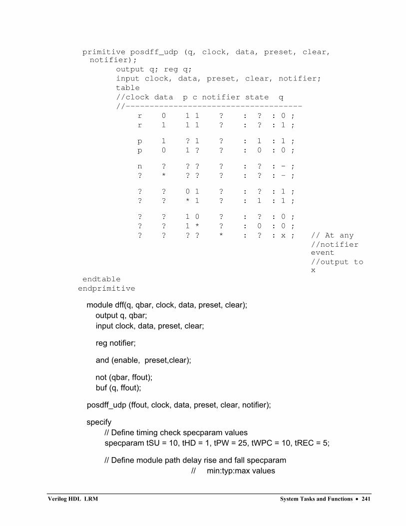
primitive posdff_udp (q, clock, data, preset, clear, notifier);
output q; reg q; input clock, data, preset, clear, notifier; table //clock data p c notifier state q //------------------------------------- r 0 1 1 ? : ? : 0 ; r 1 1 1 ? : ? : 1 ;
p 1 ? 1 ? : 1 : 1 ; p 0 1 ? ? : 0 : 0 ;
n ? ? ? ? : ? : - ; ? * ? ? ? : ? : - ;
? ? 0 1 ? : ? : 1 ; ? ? * 1 ? : 1 : 1 ;
? ? 1 0 ? : ? : 0 ; ? ? 1 * ? : 0 : 0 ; ? ? ? ? * : ? : x ; // At any //notifier
event //output to
x endtable endprimitive
module dff(q, qbar, clock, data, preset, clear); output q, qbar; input clock, data, preset, clear;
reg notifier;
and (enable, preset,clear);
not (qbar, ffout); buf (q, ffout);
posdff_udp (ffout, clock, data, preset, clear, notifier);
specify // Define timing check specparam values specparam tSU = 10, tHD = 1, tPW = 25, tWPC = 10, tREC = 5;
// Define module path delay rise and fall specparam // min:typ:max values
Verilog HDL LRM System Tasks and Functions • 241
specparam tPLHc = 4:6:9 , tPHLc = 5:8:11; specparam tPLHpc = 3:5:6 , tPHLpc = 4:7:9;
// Specify module path delays (clock *> q,qbar) = (tPLHc, tPHLc); (preset,clear *> q,qbar) = (tPLHpc, tPHLpc);
// Setup time : data to clock, only when preset and //clear are 1 $setup(data, posedge clock &&& enable, tSU, notifier);
// Hold time : clock to data, only when preset and clear are 1 $hold(posedge clock, data &&& enable, tHD, notifier);
// Clock period check $period(posedge clock, tPW, notifier);
// Pulse width : preset, clear $width(negedge preset, tWPC, 0, notifier); $width(negedge clear, tWPC, 0, notifier);
// Recovery time: clear or preset to clock $recovery(posedge preset, posedge clock, tREC, notifier); $recovery(posedge clear, posedge clock, tREC, notifier); endspecify
endmodule
Example B- 14: Notifier setting a register in response to a timing violation
It is important to remember that this model applies to edge-sensitive UDPs only; for level-sensitive models, you must generate an additional UDP for x propagation.
B.9.10 Enabling Timing Checks with Conditioned Events
A construct called a conditioned event ties the occurrence of timing checks to the value of a conditioning signal.
Syntax B-2 demonstrates the conditioned event syntax.
<controlled_timing_check_event> ::= <timing_check_event_control> <specify_terminal_descriptor> < &&&
<timing_check_condition>>?
<timing_check_condition> ::= <scalar_expression> ||= ~<scalar_expression>
Verilog HDL LRM System Tasks and Functions • 242
||= <scalar_expression>==<scalar_constant> ||= <scalar_expression>===<scalar_constant> ||= <scalar_expression>!=<scalar_constant> ||= <scalar_expression>!==<scalar_constant>
Syntax B- 2: Syntax of conditioned event
To illustrate the difference between conditioned and unconditioned timing check events, consider the following unconditioned version of the first line in Example B-15:
$setup( data, posedge clk, 10 );
Here, a setup check will occur every time there is a positive edge on signal clk.
To trigger the setup check on the positive clk edge only when signal clr is high, rewrite the command as it appears in Example B-15’s first line.
$setup( data, posedge clk &&& clr, 10 ) ;
setup( data, posedge clk &&& (~clr), 10 ) ; $setup( data, posedge clk &&& (clr===0), 10 );
Example B- 15: Example of conditioned event
The second and third lines of Example B-15 show two ways to trigger the same timing check on the positive clk edge only when clr is low.
The comparisons used in the condition may be deterministic—as in ===, !==, ~, or no operation, or non-deterministic—as in == or !=.
In the second example above, note that the comparison uses === and is therefore deterministic. When comparisons are deterministic, an x value on the conditioning signal will not enable the timing check.
For non-deterministic comparisons, an x on the conditioning signal will enable the timing check.
There are two constraints to bear in mind when using conditioned events:
1. The conditioning signal must be a scalar net; the conditioning signal cannot be a vector or expression.
2. Because conditioning signals cannot be expressions, you may use only one conditioning signal per event.
If you need more than one conditioning signal for conditioning timing checks, you can combine the appropriate logic in a separate signal outside the specify block, and then use that single signal as the conditioning signal.
For example, to perform the previous sample setup check on the positive clk edge only when clr and set are high, add the following statement outside the specify block:
Verilog HDL LRM System Tasks and Functions • 243
and( clr_and_set, clr, set );
Then, add the condition to the timing check using the signal clr_and_set as follows:
$setup( data, posedge clk &&& clr_and_set, 10 );
Verilog HDL LRM System Tasks and Functions • 244
Compiler Directives
C.0 Compiler Overview
This section describes implementation-specific compiler directives requiring standardization.
All Verilog compiler directives are preceded by the (` ) character. This character is called accent grave. It is different from the character (’), which is the single quote character. The scope of compiler directives extends from the point where it is processed, across all files processed, to the point where another compiler directive supersedes it or the processing completes. See the section on C.4 `resetall for a discussion of the impact this has on libraries.
This appendix describes the following compiler directives:
• `define
• `default_nettype
• `unconnected_drive
• `nounconnected_drive
• `resetall
• `timescale
C.1 `define
The directive `define creates macros for text substitution (see also E.7.2 Defining Variable Names to Control Conditional Compilation). It can be used both inside and outside module definitions. After a text macro is defined, it can be used in the source description by using the (`) character, followed by the macro name. The compiler will substitute the text of the macro for the string ‘macro_name.
A text macro substitution facility allows meaningful names to represent commonly used pieces of text.
The syntax for text macro definitions is as follows:
<text_macro_definition> ::=`define <text_macro_name> <MACRO_TEXT>
<text_macro_name> ::= <IDENTIFIER>
<MACRO_TEXT> is any arbitrary text up to the end of the line. Items <text_macro_name> and <MACRO_TEXT> must be specified on the same line. If a line comment (that is, a comment using the characters //) is included in the text, then the comment does not become part of the text substituted. The text for <MACRO_TEXT> may be blank, in which case the text macro is defined to be empty and no text is substituted when the macro is used.
The syntax for using a text macro is as follows:
Verilog HDL LRM Compiler Directives • 245
<text_macro_usage>::= `<text_macro_name>
Examples:
`define wordsize 8
reg [1:`wordsize] data;
`define typ_nand nand #5 //define a nand w/typical delay
`typ_nand g121 (q21, n10, n11);
The text comprising <MACRO_TEXT> must not be split across the following lexical tokens:
• comments
• numbers
• strings
• identifiers
• keywords
• double or triple character operators
For example, the following two lines are illegal specifications:
`define first_half "start of string
$display(`first_half end of string");
If you develop compiler directives, be aware of the following:
• If you implement the compiler directive `foo—and if you implement the directive `define as some tools do—then if you write `define foo, the meaning of `foo is ambiguous.
• In source written for some tools, text macro names may not be the same as compiler directive keywords.
• Text macro names can be the same as ordinary identifiers. For example, signal_name and `signal_name are different. All text macro names are put into one symbol table. Redefinition of text macros is allowed; the newest definition of a particular text macro will prevail when the macro name is used in the source text.
C.2 `default_nettype
The directive `default_nettype controls the net type created for implicit net declarations. It can be used only outside of module definitions. It affects all modules that follow the directive, even across source file boundaries. Multiple `default_nettype directives are allowed. The latest one encountered controls the type of nets that will be implicitly declared. The following is the syntax of the directive:
`default_nettype <type_of_net>
Verilog HDL LRM Compiler Directives • 246
The following are the keywords for the net types that can be specified as arguments for the directive:
wire tri tri0
wand triand tri1
wor trior trireg
When no `default_nettype directive is present, implicit nets are of type wire.
See the chapters on 3.5 Implicit Declarations and 6.9 Implicit Net Declarations for a discussion of implicit net declarations.
C.3 `unconnected_drive and `nounconnected_drive
The directive `unconnected_drive causes all unconnected input ports between it and `nounconnected_drive to be pulled up or down instead of floating to the high impedance value z. `unconnected_drive takes one of two arguments—pull1 or pull0. When pull1 is specified, all unconnected input ports are automatically pulled up. When pull0 is specified, unconnected ports are pulled down. These directives must be specified outside modules only.
C.4 `resetall
This compiler directive resets all compiler directives to the default values that are active when it is encountered during compilation. This is useful for ensuring that only those directives that are desired in compiling a particular source file are active.
The recommended usage is to place `resetall at the beginning of each source text file, followed immediately by the directives desired in the file. This directive is particularly important in library files and library directory files. `
C.5 `timescale
This directive specifies the time unit and time precision of the modules that follow it. The time unit is the unit of measurement for time values such as the simulation time and delay values. The time precision specifies how the tool rounds time values. The rounded values the tool uses are accurate to within the unit of time specified as the time precision.
Timescales let you use modules that were developed with different time units together in the same design. The tool can, for example, simulate a design that contains both a module whose delays are specified in nanoseconds and a module whose delays are specified in picoseconds.
To use modules with different time units in the same design, you need the following timescale constructs:
• the `timescale compiler directive to specify the unit of measurement for time and precision of time in the modules in your design
• the $printtimescale system task to display the time unit and precision of a module
Verilog HDL LRM Compiler Directives • 247
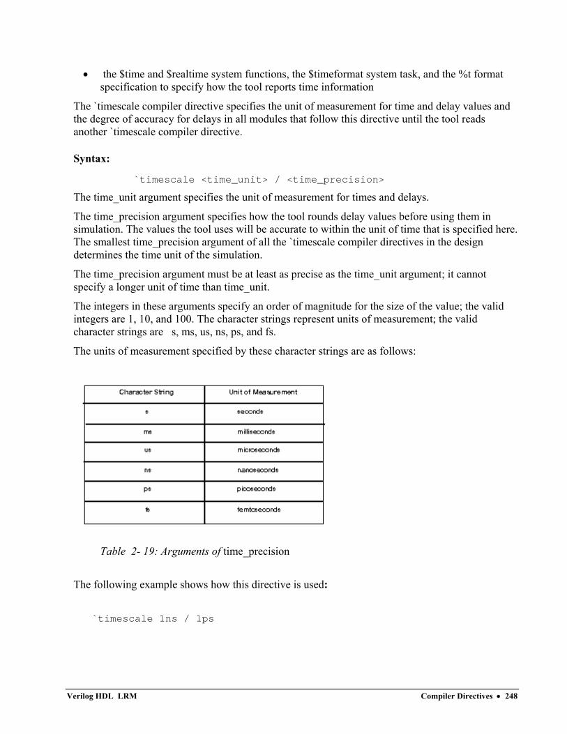
• the $time and $realtime system functions, the $timeformat system task, and the %t format specification to specify how the tool reports time information
The `timescale compiler directive specifies the unit of measurement for time and delay values and the degree of accuracy for delays in all modules that follow this directive until the tool reads another `timescale compiler directive.
Syntax:
`timescale <time_unit> / <time_precision>
The time_unit argument specifies the unit of measurement for times and delays.
The time_precision argument specifies how the tool rounds delay values before using them in simulation. The values the tool uses will be accurate to within the unit of time that is specified here. The smallest time_precision argument of all the `timescale compiler directives in the design determines the time unit of the simulation.
The time_precision argument must be at least as precise as the time_unit argument; it cannot specify a longer unit of time than time_unit.
The integers in these arguments specify an order of magnitude for the size of the value; the valid integers are 1, 10, and 100. The character strings represent units of measurement; the valid character strings are s, ms, us, ns, ps, and fs.
The units of measurement specified by these character strings are as follows:
Table 2- 19: Arguments of time_precision
The following example shows how this directive is used:
`timescale 1ns / 1ps
Verilog HDL LRM Compiler Directives • 248
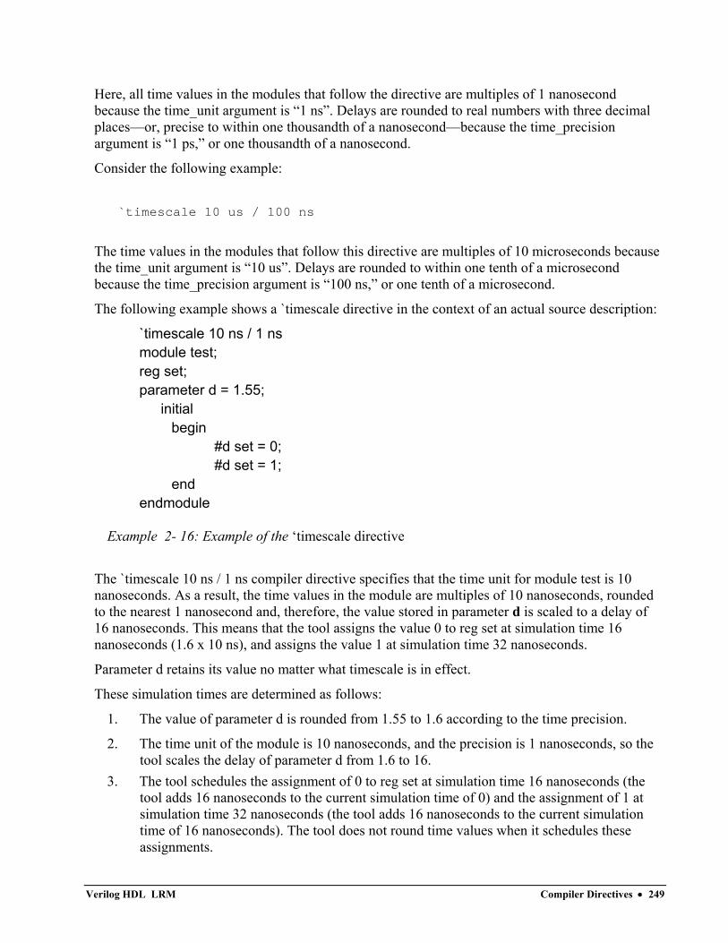
Here, all time values in the modules that follow the directive are multiples of 1 nanosecond because the time_unit argument is “1 ns”. Delays are rounded to real numbers with three decimal places—or, precise to within one thousandth of a nanosecond—because the time_precision argument is “1 ps,” or one thousandth of a nanosecond.
Consider the following example:
`timescale 10 us / 100 ns
The time values in the modules that follow this directive are multiples of 10 microseconds because the time_unit argument is “10 us”. Delays are rounded to within one tenth of a microsecond because the time_precision argument is “100 ns,” or one tenth of a microsecond.
The following example shows a `timescale directive in the context of an actual source description:
`timescale 10 ns / 1 ns module test; reg set; parameter d = 1.55; initial begin #d set = 0; #d set = 1; end endmodule
Example 2- 16: Example of the ‘timescale directive
The `timescale 10 ns / 1 ns compiler directive specifies that the time unit for module test is 10 nanoseconds. As a result, the time values in the module are multiples of 10 nanoseconds, rounded to the nearest 1 nanosecond and, therefore, the value stored in parameter d is scaled to a delay of 16 nanoseconds. This means that the tool assigns the value 0 to reg set at simulation time 16 nanoseconds (1.6 x 10 ns), and assigns the value 1 at simulation time 32 nanoseconds.
Parameter d retains its value no matter what timescale is in effect.
These simulation times are determined as follows:
1. The value of parameter d is rounded from 1.55 to 1.6 according to the time precision.
2. The time unit of the module is 10 nanoseconds, and the precision is 1 nanoseconds, so the tool scales the delay of parameter d from 1.6 to 16.
3. The tool schedules the assignment of 0 to reg set at simulation time 16 nanoseconds (the tool adds 16 nanoseconds to the current simulation time of 0) and the assignment of 1 at simulation time 32 nanoseconds (the tool adds 16 nanoseconds to the current simulation time of 16 nanoseconds). The tool does not round time values when it schedules these assignments.
Verilog HDL LRM Compiler Directives • 249
List of System Task and System Function Keywords
D.0 System Tasks Overview
The following is a list of some of the keywords currently used by tools for names of system tasks and system functions, with a brief description of each keyword. See Appendix B, System Tasks and Functions, for descriptions of some frequently used tasks and functions.
$bitstoreal
$countdrivers
$display
$fclose
$fdisplay
$fmonitor
$fopen
$fstrobe
$fwrite
$finish
$getpattern
$history
$incsave
$input
$itor
$key
$list
$log
$monitor
$monitoroff
$monitoron
$nokey
$nolog
$printtimescale
$readmemb
Verilog HDL LRM 250 • List of System Task and System Function Keywords
$readmemh
$realtime
$realtobits
$reset
$reset_count
$reset_value
$restart
$rtoi
$save
$scale
$scope
$showscopes
$showvariables
$showvars
$sreadmemb
$sreadmemh
$stime
$stop
$strobe
$time
$timeformat
$write
D.1 $bitstoreal
See Appendix B, B.8 Functions and Tasks for Reals, for details.
D.2 $countdrivers
Syntax:
$countdrivers(net, net_is_forced, number_of_01x_drivers, number_of_0_drivers, number_of_1_drivers, number_of_x_drivers);
Verilog HDL LRM 251 • List of System Task and System Function Keywords
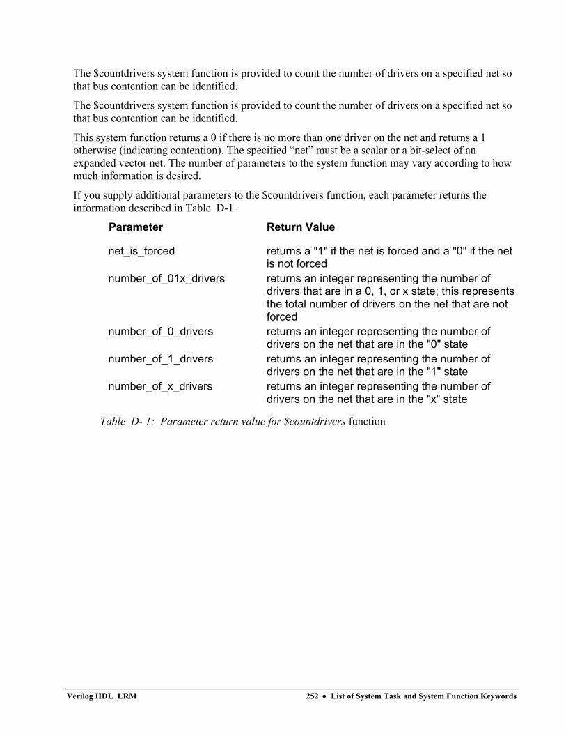
The $countdrivers system function is provided to count the number of drivers on a specified net so that bus contention can be identified.
The $countdrivers system function is provided to count the number of drivers on a specified net so that bus contention can be identified.
This system function returns a 0 if there is no more than one driver on the net and returns a 1 otherwise (indicating contention). The specified “net” must be a scalar or a bit-select of an expanded vector net. The number of parameters to the system function may vary according to how much information is desired.
If you supply additional parameters to the $countdrivers function, each parameter returns the information described in Table D-1.
Parameter Return Value
net_is_forced returns a "1" if the net is forced and a "0" if the net is not forced
number_of_01x_drivers returns an integer representing the number of drivers that are in a 0, 1, or x state; this represents the total number of drivers on the net that are not forced
number_of_0_drivers returns an integer representing the number of drivers on the net that are in the "0" state
number_of_1_drivers returns an integer representing the number of drivers on the net that are in the "1" state
number_of_x_drivers returns an integer representing the number of drivers on the net that are in the "x" state
Table D- 1: Parameter return value for $countdrivers function
Verilog HDL LRM 252 • List of System Task and System Function Keywords
D.3 $display
See Appendix B, B.1 The Display and Write Tasks, for details.
D.4 Value Change Dump File Tasks
Seven system tasks are provided to create and format the value change dump file.
Syntax:
$dumpfile(<filename>);
$dumpvars(<levels> <,<module|var>>* );
$dumpoff;
$dumpon;
$dumpall;
$dumplimit(<filesize>);
$dumpflush;
The $dumpfile system task specifies the name of the value change dump file.
The $dumpvars system task specifies the variables whose changing values a tool records in the value change dump file. The $dumpvars when invoked with no arguments dumps all variables in the design.
The $dumpoff system task stops a tool from recording value changes in the value change dump file.
The $dumpon system task allows a tool to resume recording value changes in the value change dump file.
The $dumpall system task creates a checkpoint that shows the current value of all variables being recorded in the value change dump file.
The $dumplimit system task sets the size of the value change dump file.
The $dumpflush system task empties the dump file buffer and ensures that all the data in that buffer is stored in the value change dump file.
D.5 File Output
Each of the four formatted display tasks—$display, $write, $monitor, and $strobe—has a counterpart that writes to specific files as opposed to the log file and standard output. These counterpart tasks—$fdisplay, $fwrite, $fmonitor, and $fstrobe—accept the same type of parameters as the tasks they are based upon, with one exception: The first parameter must be a multichannel descriptor that indicates where to direct the file output. A multichannel descriptor is either a variable or the result of an expression that takes the form of a 32-bit unsigned integer value. This value determines which open files the task will write to.
Verilog HDL LRM 253 • List of System Task and System Function Keywords
Syntax:
$fdisplay(<multi_channel_descriptor>, P1, P2, ... , Pn);
$fwrite(<multi_channel_descriptor>, P1, P2, ... , Pn);
$fstrobe(<multi_channel_descriptor>, P1, P2, ..., Pn);
$fmonitor(<multi_channel_descriptor>, P1, P2, ..., Pn);
$fopen("<name_of_file>")
$fclose(<multichannel_descriptor>);
The function $fopen opens the file specified as a parameter and returns a 32-bit unsigned multichannel descriptor that is uniquely associated with the file. It returns 0 if the file could not be opened for writing.
The multichannel descriptor should be thought of as a set of 32 flags, where each flag represents a single output channel. The least significant bit (bit 0) of a multichannel descriptor always refers to the standard output—that is, the log file and the screen (unless it has been redirected to a file). The standard output is also called channel 0. The other bits refer to channels that have been opened by the $fopen system function.
The first call to $fopen opens channel 1 and returns a multichannel descriptor value of 2—that is, bit 1 of the descriptor is set. A second call to $fopen opens channel 2 and returns a value of 4—that is, only bit 2 of the descriptor is set. Subsequent calls to $fopen open channels 3, 4, 5, and so on and returns values of 8, 16, 32, and so on, up to a maximum of 31 channels. Thus, a channel number corresponds to an individual bit in a multichannel descriptor.
The advantage of multichannel descriptors is that they allow a single system task to write the same information to multiple outputs simultaneously. This is accomplished by setting more than one bit in the multichannel descriptor, and can be done by combining the values returned by $fopen in a bit-wise OR operation. Another advantage of multichannel descriptors is that it is easy to set up descriptions where the channels that receive diagnostic information can be dynamically altered during simulation, and even controlled in interactive commands.
Note that the number of simultaneous output channels that may be active at any one time is dependent on the operating system and is not determined by the tool.
The $fclose system task closes the channels specified in the multichannel descriptor, and does not allow any further output to the closed channels. The $fopen task will reuse channels that have been closed.
Example D-1 shows how to set up multichannel descriptors. In this example, three different channels are opened using the $fopen function. The three multichannel descriptors that are returned by the function are then combined in a bit-wise OR operation and assigned to the integer variable messages. The messages variable can then be used as the first parameter in a file output task to direct output to all three channels at once. To create a descriptor that directs output to the standard output as well, the messages variable is bit-wise ORed with the constant 1, which effectively enables channel 0.
integer messages,
Verilog HDL LRM 254 • List of System Task and System Function Keywords
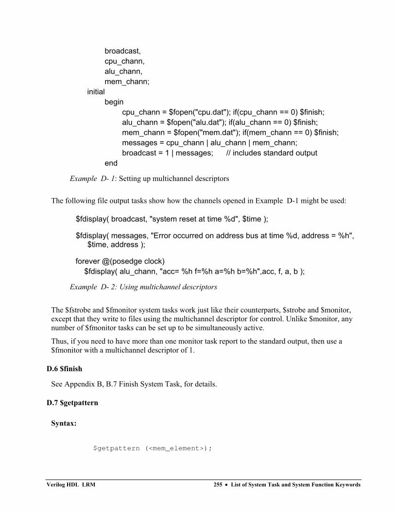
broadcast, cpu_chann, alu_chann, mem_chann; initial begin cpu_chann = $fopen("cpu.dat"); if(cpu_chann == 0) $finish; alu_chann = $fopen("alu.dat"); if(alu_chann == 0) $finish; mem_chann = $fopen("mem.dat"); if(mem_chann == 0) $finish; messages = cpu_chann | alu_chann | mem_chann; broadcast = 1 | messages; // includes standard output end
Example D- 1: Setting up multichannel descriptors
The following file output tasks show how the channels opened in Example D-1 might be used:
$fdisplay( broadcast, "system reset at time %d", $time );
$fdisplay( messages, "Error occurred on address bus at time %d, address = %h", $time, address );
forever @(posedge clock) $fdisplay( alu_chann, "acc= %h f=%h a=%h b=%h",acc, f, a, b );
Example D- 2: Using multichannel descriptors
The $fstrobe and $fmonitor system tasks work just like their counterparts, $strobe and $monitor, except that they write to files using the multichannel descriptor for control. Unlike $monitor, any number of $fmonitor tasks can be set up to be simultaneously active.
Thus, if you need to have more than one monitor task report to the standard output, then use a $fmonitor with a multichannel descriptor of 1.
D.6 $finish
See Appendix B, B.7 Finish System Task, for details.
D.7 $getpattern
Syntax:
$getpattern (<mem_element>);
Verilog HDL LRM 255 • List of System Task and System Function Keywords
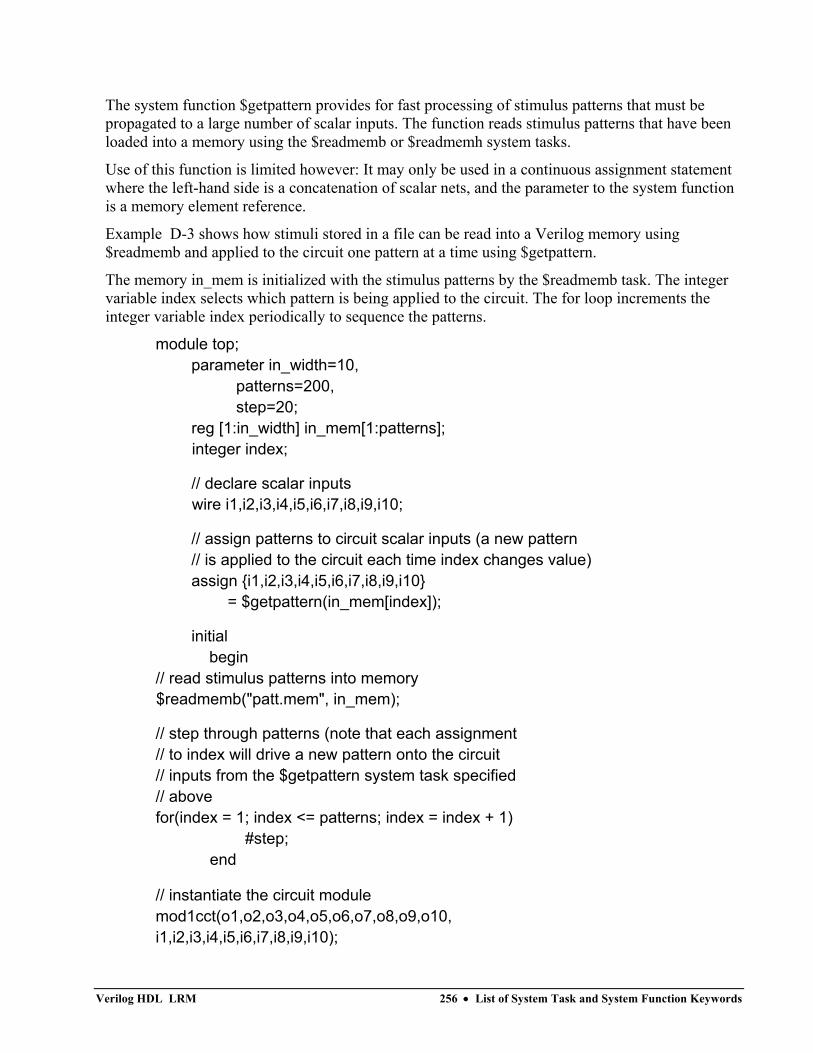
The system function $getpattern provides for fast processing of stimulus patterns that must be propagated to a large number of scalar inputs. The function reads stimulus patterns that have been loaded into a memory using the $readmemb or $readmemh system tasks.
Use of this function is limited however: It may only be used in a continuous assignment statement where the left-hand side is a concatenation of scalar nets, and the parameter to the system function is a memory element reference.
Example D-3 shows how stimuli stored in a file can be read into a Verilog memory using $readmemb and applied to the circuit one pattern at a time using $getpattern.
The memory in_mem is initialized with the stimulus patterns by the $readmemb task. The integer variable index selects which pattern is being applied to the circuit. The for loop increments the integer variable index periodically to sequence the patterns.
module top; parameter in_width=10, patterns=200, step=20; reg [1:in_width] in_mem[1:patterns]; integer index;
// declare scalar inputs wire i1,i2,i3,i4,i5,i6,i7,i8,i9,i10;
// assign patterns to circuit scalar inputs (a new pattern // is applied to the circuit each time index changes value) assign {i1,i2,i3,i4,i5,i6,i7,i8,i9,i10} = $getpattern(in_mem[index]);
initial begin // read stimulus patterns into memory $readmemb("patt.mem", in_mem);
// step through patterns (note that each assignment // to index will drive a new pattern onto the circuit // inputs from the $getpattern system task specified // above for(index = 1; index <= patterns; index = index + 1) #step; end
// instantiate the circuit module mod1cct(o1,o2,o3,o4,o5,o6,o7,o8,o9,o10, i1,i2,i3,i4,i5,i6,i7,i8,i9,i10);
Verilog HDL LRM 256 • List of System Task and System Function Keywords
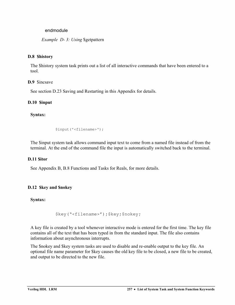
endmodule
Example D- 3: Using $getpattern
D.8 $history
The $history system task prints out a list of all interactive commands that have been entered to a tool.
D.9 $incsave
See section D.23 Saving and Restarting in this Appendix for details.
D.10 $input
Syntax:
$input("<filename>");
The $input system task allows command input text to come from a named file instead of from the terminal. At the end of the command file the input is automatically switched back to the terminal.
D.11 $itor
See Appendix B, B.8 Functions and Tasks for Reals, for more details.
D.12 $key and $nokey
Syntax:
$key(“<filename>”);$key;$nokey;
A key file is created by a tool whenever interactive mode is entered for the first time. The key file contains all of the text that has been typed in from the standard input. The file also contains information about asynchronous interrupts.
The $nokey and $key system tasks are used to disable and re-enable output to the key file. An optional file name parameter for $key causes the old key file to be closed, a new file to be created, and output to be directed to the new file.
Verilog HDL LRM 257 • List of System Task and System Function Keywords
D.13 $list
Syntax:
$list;$list (<name>);
When invoked without a parameter, $list produces a listing of the module, task, function, or named block that is defined as the current scope setting. If an optional parameter is supplied, it must refer to a specific module, task, function or named block, in which case the specified object will be listed.
D.14 $log and $nolog
Syntax:
$log(“<filename>”);$log;$nolog;
Tools may create a log file that contains a copy of all the text that is printed to the standard output. The log file may also contain, at the beginning of the file, the host command that was used to run the tool.
The $nolog and $log system tasks are used to disable and re-enable output to the log file. The $nolog task disables output to the log file, while the $log task re-enables the output. An optional file name parameter for $log causes the old file to be closed, a new log file to be created, and output to be directed to the new log file.
D.15 $monitor, $monitoron, $monitoroff
See Appendix B, B.3 Continuous Monitoring, for details.
D.16 $printtimescale
See Appendix B, B.5.1 The $printtimescale System Task, for details.
D.17 $readmemb and $readmemh
Syntax:
$readmemb("<filename>", <memname>);
$readmemb("<filename>", <memname>, <start_addr>);
$readmemb("<filename>", <memname>, <start_addr>, <finish_addr>);
$readmemh("<filename>", <memname>);$readmemh("<filename>", <memname>, <start_addr>);
Verilog HDL LRM 258 • List of System Task and System Function Keywords
$readmemh("<filename>", <memname>, <start_addr>, <finish_addr>);
Two system tasks—$readmemb and $readmemh—read and load data from a specified text file into a specified memory. Either task may be executed at any time during simulation. The text file to be read must contain only the following:
• white space (spaces, new lines, tabs, and form-feeds)
• comments (both types of comment are allowed)
• binary or hexadecimal numbers
The numbers must have neither the length nor the base format specified. For $readmemb, each number must be binary. For $readmemh, the numbers must be hexadecimal. The unknown value (x or X), the high impedance value (z or Z), and the underscore (_) can be used in specifying a number as in a Verilog source description. White space and/or comments must be used to separate the numbers.
In the following discussion, the term “address” refers to an index into the array that models the memory.
As the file is read, each number encountered is assigned to a successive word element of the memory. Addressing is controlled both by specifying start and/or finish addresses in the system task invocation, and by specifying addresses in the data file.
When addresses appear in the data file, the format is an “at” character (@) followed by a hexadecimal number as follows:
@hh...h
Both upper and lower case digits are allowed in the number. No white space is allowed between the @ and the number. You may use as many address specifications as you need within the data file. When the system task encounters an address specification, it loads subsequent data starting at that memory address.
If no addressing information is specified within the system task, and no address specifications appear within the data file, then the default start address is the left-hand address given in the declaration of the memory, and consecutive words are loaded until either the memory is full or the data file is completely read. If the start address is specified in the task without the finish address, then loading starts at the specified start address and continues towards the right-hand address given in the declaration of the memory.
If both start and finish addresses are specified as parameters to the task, then loading begins at the start address and continues toward the finish address, regardless of how the addresses are specified in the memory declaration.
When addressing information is specified both in the system task and in the data file, the addresses in the data file must be within the address range specified by the system task parameters, otherwise an error message is issued and the load operation is terminated.
Verilog HDL LRM 259 • List of System Task and System Function Keywords
A warning message is issued if the number of data words in the file differs from the number of words in the range implied by the start and finish addresses.
For example, consider the following declaration of memory mem:
reg[7:0] mem[1:256];
Given this declaration, each of the following statements will load data into mem in a different manner:
initial $readmemh("mem.data", mem);initial $readmemh("mem.data", mem, 16);initial $readmemh("mem.data", mem, 128, 1);
The first statement will load up the memory at simulation time 0 starting at the memory address 1. The second statement will begin loading at address 16 and continue on towards address 256. For the third and final statement, loading will begin at address 128 and continue down towards address 1.
In the third case, when loading is complete, a final check is performed to ensure that exactly 128 numbers are contained in the file. If the check fails, a tool issues a warning message.
D.18 $realtime
See $time in Appendix B.4.2 The $realtime System Function for details.
D.19 $realtobits
See Appendix B, B.8 Functions and Tasks for Reals, for details.
D.20 $reset, $reset_count and $reset_value
The $reset system task enables a tool to be reset to its “Time 0” state so that processing (e.g., simulation) can begin again.
The $reset_count system function keeps track of the number of times the tool is reset. The $reset_value system function returns the value specified by the reset_value parameter argument to the $reset system task. The $reset_value system function is used to communicate information from before a reset of a tool to the time 0 state to after the reset.
The following are some of the simulation methods that you can employ with this system task and these system functions:
• determine the force statements your design needs to operate correctly, reset the simulation time to 0, enter these force statements, and start to simulate again
• reset the simulation time to 0 and apply new stimuli
Verilog HDL LRM 260 • List of System Task and System Function Keywords
• determine that debug system tasks, such as $monitor and $strobe, are keeping track of the correct nets or registers, reset the simulation time to 0, and begin simulation again
The $reset system task tells a tool (for example a simulator) to return the processing of your design to its logical state at time 0. When a tool executes the $reset system task, it takes the following actions to stop the process (e.g., simulation):
• disables all concurrent activity, initiated in either initial and always procedural blocks in the source description or through interactive mode (disables, for example, all force and assign statements, the current $monitor system task, and any other active task)
• cancels all scheduled simulation events
After a simulation tool executes the $reset system task, the simulation is in the following state:
• The simulation time is 0.
• All registers and nets contain their initial values.
• The tool begins to execute the first procedural statements in all initial and always blocks.
Syntax: $reset;
$reset(<stop_value>);
$reset(<stop_value>,<reset_value>);
$reset(<stop_value>,<reset_value>,<diagnostics_value>);
The stop_value argument
The stop_value argument indicates whether interactive mode or processing is entered immediately after resetting of the tool. A value of 0 or no argument causes interactive mode to be entered after resetting the tool. A non-zero value passed to $reset causes the tool to begin processing immediately.
The reset_value argument
The reset_value is an integer that you specify whose value is returned by the $reset_value system function after you reset the tool. You cannot declare an integer that keeps its value after a reset. All declared integers return to their initial value after reset, but entering an integer as this argument allows you to access what its value was before the reset with the $reset_value system function. This argument provides you with a means of communicating information from before the reset of a tool to after the reset of the tool.
The diagnostic_value argument
The diagnostic_value is the third argument. It specifies the kind of diagnostic messages a tool displays before it resets the time to 0. Increasing integer values result in increased information. A value of zero results in no diagnostic message.
Verilog HDL LRM 261 • List of System Task and System Function Keywords
D.21 $restart
See section D.23 Saving and Restarting for details.
D.22 $rtoi
See Appendix B, B.8 Functions and Tasks for Reals, for details.
D.23 Saving and Restarting
Three system tasks, $save, $restart, and $incsave, work in conjunction with one another to save the complete state of a tool into a permanent file such that the tool state can be reloaded at a later time and the tool can continue processing where it left off.
Syntax:
$save("<name_of_file>");
$restart("<name_of_file>");
$incsave("<incremental_filename>");
These system tasks work in conjunction with one another to save the complete state of a tool into a permanent file such that the tool state can be reloaded at a later time and the tool can continue processing where it left off.They are often used during long runs of a tool to save checkpoint versions of the internal state at regular intervals. They are also useful to perform quick “try and see” experiments without having to repeat the entire processing each time.
All three system tasks take a file name as a parameter. The file name must be supplied as a string enclosed in quotation marks.
The $save system task saves the complete state into the host operating system file specified as a parameter.
The $incsave system task saves only what has changed since the last invocation of $save. It is not possible to do an incremental save on any file other than the one produced by the last $save.
The $restart system task restores a previously saved state from a specified file. The state description to be restarted does not have to be related in any way to the description being replaced.
It should be noted that interactive commands are also saved by the $save task; thus, when you use $restart to restore a tool’s state, you also replace the current set of commands with the saved set of commands.
D.23.1 Incremental Save and Restart
Restarting from an incremental save is similar to restarting from a full save, except that the name of the incremental save file is specified in the restart command. The full save file that the incremental save file was based upon must still be present, as it is required for a successful restart. If the full save file has been changed in any way since the incremental save was performed, errors will result.
Verilog HDL LRM 262 • List of System Task and System Function Keywords
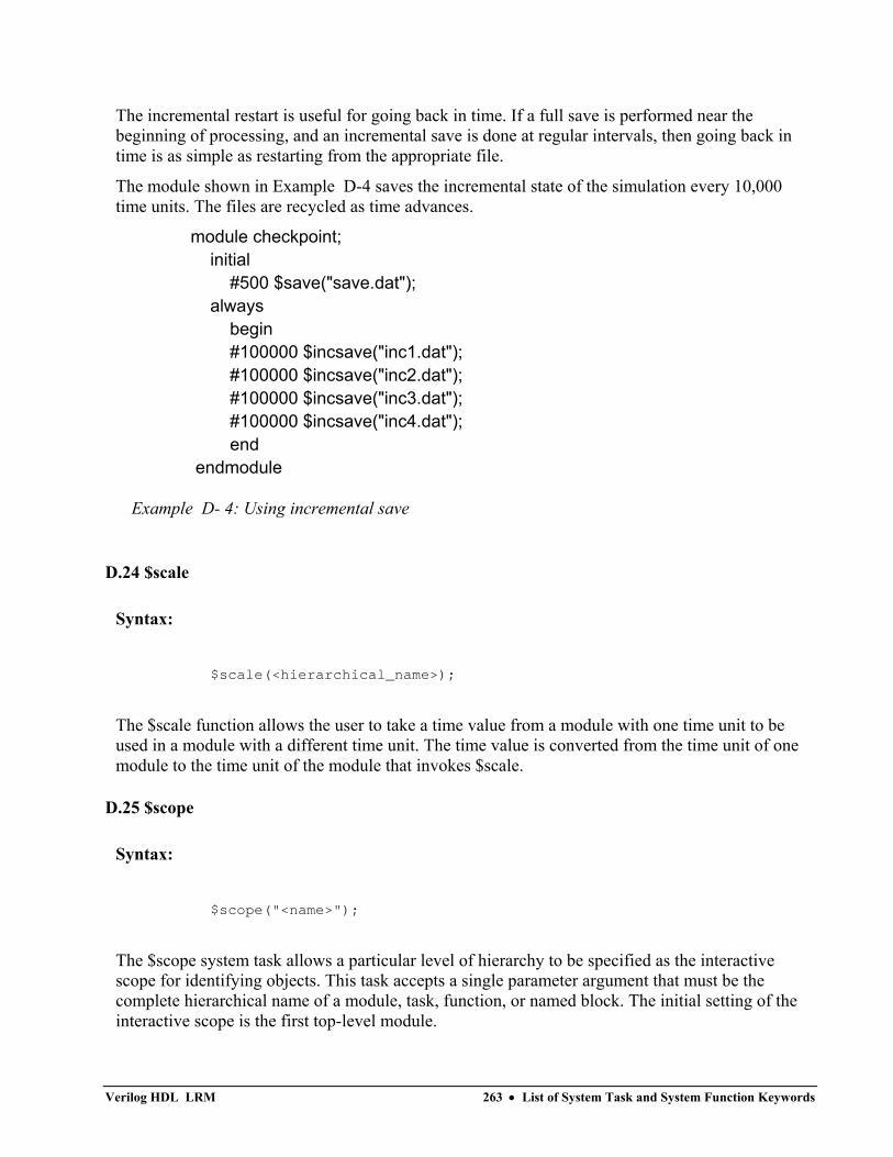
The incremental restart is useful for going back in time. If a full save is performed near the beginning of processing, and an incremental save is done at regular intervals, then going back in time is as simple as restarting from the appropriate file.
The module shown in Example D-4 saves the incremental state of the simulation every 10,000 time units. The files are recycled as time advances.
module checkpoint; initial #500 $save("save.dat"); always begin #100000 $incsave("inc1.dat"); #100000 $incsave("inc2.dat"); #100000 $incsave("inc3.dat"); #100000 $incsave("inc4.dat"); end endmodule
Example D- 4: Using incremental save
D.24 $scale
Syntax:
$scale(<hierarchical_name>);
The $scale function allows the user to take a time value from a module with one time unit to be used in a module with a different time unit. The time value is converted from the time unit of one module to the time unit of the module that invokes $scale.
D.25 $scope
Syntax:
$scope("<name>");
The $scope system task allows a particular level of hierarchy to be specified as the interactive scope for identifying objects. This task accepts a single parameter argument that must be the complete hierarchical name of a module, task, function, or named block. The initial setting of the interactive scope is the first top-level module.
Verilog HDL LRM 263 • List of System Task and System Function Keywords
D.26 $showscopes
Syntax:
$showscopes;$showscopes(n);
The $showscopes system task produces a complete list of modules, tasks, functions, and named blocks that are defined at the current scope level. An optional integer parameter can be given to $showscopes. A nonzero parameter causes all the modules, tasks, functions and named blocks in or below the current hierarchical scope to be listed. No parameter or a zero results in only objects at the current scope level to be listed.
D.27 $showvars
Syntax:
$showvars;$showvars(<list_of_variables>);
The $showvars system task produces status information for register and net variables, both scalar and vector. When invoked without parameters, $showvars displays the status of all variables in the current scope. When invoked with a <list_of_variables>, $showvars shows only the status of the specified variables. If the <list_of_variables> includes a bit-select or part-select of a register or net then the status information for all the bits of that register or net are displayed.
The system task $showvariables displays information similar to that of $showvars, but allows more control over the information displayed.
D.28 $sreadmemb and $sreadmemh
Syntax:
$sreadmemb(<mem_name>,<start_addr>,<finish_addr>, <string1>,<string2>,,,);
$sreadmemh(<mem_name>,<start_addr>,<finish_addr>, <string1>,<string2>,,,);
Where:
<mem_name> name of the memory structure
<start_addr> memory start address
<finish_addr> memory end address
Verilog HDL LRM 264 • List of System Task and System Function Keywords
<stringN> the string value containing the actual data to be placed into memory, beginning at <start_addr>
The system tasks $sreadmemb and $sreadmemh load data into memory from a Verilog source character string.
The $sreadmemh and $sreadmemb system tasks take memory data values and addresses as string arguments. These strings take the same format as the strings that appear in the input files passed as arguments to $readmemb and $readmemh.
D.29 $stime
See $time in Appendix B.4.1 The $time System Function for details.
D.30 $stop
Syntax:
$stop;
$stop(n);
The $stop system task puts the tool (for example a simulator) into halt mode, issues an interactive command prompt, and passes control to the user. This task takes an optional expression parameter (0, 1, or 2) that determines what type of diagnostic message is printed. The amount of diagnostic messages output increases with the value of the optional parameter passed to $stop.
D.31 $strobe
See Appendix B, B.2 Strobed Monitoring, for details.
D.32 $time, $stime and $realtime
See $time in Appendix B.4.1 The $time System Function, B.4.2 The $realtime System Function, and B.6 Simulation Time—The $time Function for details.
D.33 $timeformat
See Appendix B, B.5.2 The $timeformat System Task for details.
D.34 $write
See Appendix B, B.1 The Display and Write Tasks, for details.
Verilog HDL LRM 265 • List of System Task and System Function Keywords
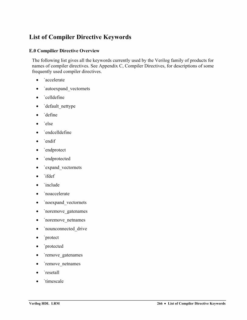
List of Compiler Directive Keywords
E.0 Compilier Directive Overview
The following list gives all the keywords currently used by the Verilog family of products for names of compiler directives. See Appendix C, Compiler Directives, for descriptions of some frequently used compiler directives.
• `accelerate
• `autoexpand_vectornets
• `celldefine
• `default_nettype
• `define
• `else
• `endcelldefine
• `endif
• `endprotect
• `endprotected
• `expand_vectornets
• `ifdef
• `include
• `noaccelerate
• `noexpand_vectornets
• `noremove_gatenames
• `noremove_netnames
• `nounconnected_drive
• `protect
• `protected
• `remove_gatenames
• `remove_netnames
• `resetall
• `timescale
Verilog HDL LRM 266 • List of Compiler Directive Keywords
• `unconnected_drive
E.1 `accelerate and `noaccelerate
The directive `accelerate results in an acceleration algorithm being applied to modules following the directive. There is also a `noaccelerate directive that causes those modules which follow to use a normal algorithm.
These directives can only be specified outside the module definitions. Any number of these directives may appear in the source description.
E.2 `autoexpand_vectornets
This directive lets the compiler expand vectors as needed to form proper connections between elements of the description.
This directive may only appear outside a module boundary.
E.3 `celldefine and `endcelldefine
The directives `celldefine and `endcelldefine tag modules as cell modules. Cells are used by certain PLI routines for applications such as delay calculations. It is advisable to pair each `celldefine with an `endcelldefine. More than one of these pairs may appear in a single source description.
These directives may appear anywhere in the source description but it is recommended that the directives are specified outside the module definition.
E.4 `default_nettype
See Appendix C, C.2 `default_nettype, for details.
E.5 `define
See Appendix C, C.1 `define, for details.
E.6 `expand_vectornets
This directive causes all vector nets to be expanded into a group of scalar nets, except those with the keyword vectored in their declarations.
This directive may only appear outside a module boundary.
E.7 `ifdef, `else, `endif
These conditional compilation compiler directives are used to optionally include lines of a Verilog HDL source description during compilation. The `ifdef compiler directive checks for the definition of a variable name. If the variable name is defined then the lines following the `ifdef directive are included. If the variable name is not defined and an `else directive exists then this source is compiled.
Verilog HDL LRM 267 • List of Compiler Directive Keywords
Note: SILOS III has a reserved keyword “silos” that is always true. This enables you to enclose Silos specific code and commands with a `ifdef … `else … `endif compiler directive so they can be run in SILOS III but not other simulators or synthesis tools.
These directives may appear anywhere in the source description.
Situations where the `ifdef, `else, and `endif compiler directives may be useful include:
• selecting different representations of a module such as behavioral, structural, or switch level
• choosing different timing or structural information
• selecting different stimulus for a given run of a tool
Syntax:
The `ifdef, `else, and `endif compiler directives have the following syntax:
`ifdef <text_macro_name>
<first_group_of_lines>
`else
<second_group_of_lines>
`endif
The text_macro_name is a Verilog HDL identifier. The first_group_of_lines and second_group_of_lines are any parts of a Verilog HDL source description. The `else compiler directive and second_group_of_lines are optional.
The `ifdef, `else, and `endif compiler directives work in the following manner:
• When an `ifdef is encountered, the text_macro_name is tested to see if it is defined as a text macro name using `define within the Verilog HDL source description.
• If the text_macro_name is defined, the first_group_of_lines is compiled as part of the description. If there is an `else compiler directive, the second_group_of_lines is ignored.
• If the text_macro_name has not been defined, the first_group_of_lines is ignored. If there is an `else compiler directive the second_group_of_lines is compiled.
Example E-1 shows the `ifdef, `else, and `endif compiler directives in a module.
module and_op (a, b, c);
output a;
input b, c;
`ifdef behavioral
wire a = b & c;
`else
Verilog HDL LRM 268 • List of Compiler Directive Keywords
and (a,b,c);
`endif
endmodule
Example E- 1: An example of the conditional compilation specification
Syntax checking
Any group of lines that the compiler ignores still must follow the Verilog HDL lexical conventions for white space, comments, numbers, strings, identifiers, keywords, and operators.
E.7.1 Nesting the `ifdef, `else, and `endif Compiler Directives
You can nest the `ifdef, `else, and `endif compiler directives as shown in Example E-2.
module test(out); output out; `define wow `define nest_one `define second_nest `define nest_two `ifdef wow initial $display("wow is defined"); `ifdef nest_one initial $display("nest_one is defined"); `ifdef nest_two initial $display("nest_two is defined"); `else initial $display("nest_two is not defined"); `endif `else initial $display("nest_one is not defined"); `endif `else initial $display("wow is not defined"); `ifdef second_nest initial $display("nest_two is defined"); `else initial $display("nest_two is not defined"); `endif `endif endmodule
Verilog HDL LRM 269 • List of Compiler Directive Keywords
Example E- 2: Nested `ifdef, `else, and `endif compiler directives
E.7.2 Defining Variable Names to Control Conditional Compilation
The `ifdef variables are defined using the compiler directive (`define) to define a text macro.
The `define compiler directive
The `define compiler directive allows you to create macros for text substitution (see also C.1 `define). Text macros may be placed both inside and outside module definitions. When a tool encounters the `ifdef compiler directive, it checks to see if its variable name matches a text macro name in a `define compiler directive. The syntax for this usage of the `define compiler directive is as follows:
`define <text_macro_name> [<macro_contents>]
E.8 `include
The file inclusion (`include) compiler directive is used to insert the entire contents of a source file in another file during compilation. The result is as though the contents of the included source file appear in place of the `include command. The `include compiler directive can be used to include global or commonly used definitions and tasks without encapsulating repeated code within module boundaries.
Advantages of using the `include compiler directive include the following:
• providing an integral part of configuration management
• improving the organization of Verilog HDL source descriptions
• facilitating the maintenance of Verilog HDL source descriptions
Syntax:
The syntax for the `include compiler directive is as follows:
`include "<filename>"
The compiler directive `include can be specified anywhere within the Verilog HDL description. The <filename> is the name of the file to be included in the source file. The <filename> can be a full or relative path name, as in the following example:
`include "parts/count.v"
Verilog HDL LRM 270 • List of Compiler Directive Keywords
Only white space or a comment may appear on the same line as the `include compiler directive. Examples of legal comments for the `include compiler directive are as follows:
`include "fileB"`include "fileB" // including fileB
Nested `include Compiler Directives An `include file can contain other `include compiler directives. Recursive `include directives are considered an error.
E.9 `noexpand_vectornets
This directive causes no expansion to take place except where explicitly specified by the keyword scalared in a vector net declaration.
This directive may only appear outside a module boundary.
E.10 `protect and `endprotect
These directives are used to mark regions in a source description that will be processed by a tool into an intermediate form. This allows proprietary Verilog source descriptions to be protected from being accessed or modified.
These directives may appear anywhere in the source description.
E.11 `protected and `endprotected
The directive `protected and `endprotected bound a region once it has been compiled into a protected form.
A tool is passed a file containing a Verilog source description with the directives `protect and `endprotect. After processing, a new source file is created that differs from the original file in two ways:
• the directive `protect and `endprotect become `protected and `endprotected respectively.
• the regions marked for protection in the original source description become unreadable.
E.12 `remove_gatenames and `noremove_gatenames
The directive `remove_gatenames causes any gate instance names that have been specified in modules affected by this directive to be eliminated from the second and all subsequent instances of each module. This directive cannot be used if it is necessary to refer to gates by hierarchical name. The directive `noremove_gatenames stops the elimination of gate names.
These directives must be specified outside the module definition. All the modules between `remove_gatenames and `noremove_gatenames are affected.
Verilog HDL LRM 271 • List of Compiler Directive Keywords
E.13 `remove_netnames and `noremove_netnames
The directive `remove_netnames causes any net names that have been specified in modules affected by this directive to be eliminated from the second and all subsequent instances of each module. This directive cannot be used if it is necessary to refer to nets by hierarchical name. The directive `noremove_netnames stops the elimination of names.
These directives must be specified outside of modules. All modules between `remove_netnames and `noremove_netnames are affected.
E.14 `resetall
See Appendix C, C.4 `resetall, for details.
E.15 `timescale
See Appendix C, C.5 `timescale, for details.
E.16 `unconnected_drive and `nounconnected_drive
The directive `unconnected_drive causes unconnected input ports to be automatically pulled up (if pull1 is specified) or down (if pull0 is specified) instead of floating to the high impedance value z. Inputs are pulled up or down in all modules between the directives `unconnected_drive and `nounconnected_drive.
This directive may only appear outside a module boundary.
Verilog HDL LRM 272 • List of Compiler Directive Keywords
List of Keywords
Keywords
Keywords are pre-defined non-escaped identifiers which define the language constructs. An escaped identifier is never treated as a keyword. All keywords are defined in lower-case unless the upper-case option is used when compiling.
always
and
assign (see also assign)
begin
buf
bufif0
bufif1
case
casex
casez
cmos
deassign
default
defparam
disable
edge
else
end
endcase
endmodule
endfunction
endprimitive
endspecify
endtable
endtask
event
for
force
forever
fork
function
highz0
highz1
273 • List of Keywords Verilog HDL LRM
if
initial
inout
input
integer
join
large
macromodule
medium
module
nand
negedge
nmos
nor
not
notif0
notif1
or
output
parameter
pmos
posedge
primitive
pull0
pull1
pullup
pulldown
rcmos
reg
release
repeat
rnmos
rpmos
rtran
rtranif0
rtranif1
scalared
small
specify
specparam
274 • List of Keywords Verilog HDL LRM
strength
strong0
strong1
supply0
supply1
table
task
time
tran
tranif0
tranif1
tri
tri0
tri1
triand
trior
trireg
vectored
wait
wand
weak0
weak1
while
wire
wor
xnor
xor
275 • List of Keywords Verilog HDL LRM
Index
i -
in state table 93
! !
compared to ‘==0’ 38 logical negation operator 38
" ""
null string 47
$ $bitstoreal 166, 234 $countdrivers 255
syntax 255 $display 225
compared to $monitor 226 compared to $write 218 escape sequences 219 size of displayed data 222 syntax 218
$dumpall 256 $dumpfile 256 $dumpflush 256 $dumplimit 256 $dumpoff 256 $dumpon 256 $dumpvars 256 $fclose 258
syntax 257 $fdisplay 258
syntax 257 $finish 233
syntax 233 $fmonitor 258
syntax 257 $fopen 258
syntax 257 $fstrobe 258
syntax 257 $fwrite 258
syntax 257 $getpattern 259 $hold 236 $incsave
syntax 265
$input syntax 260
$itor 234 $keepcommands 260 $list
syntax 261 $monitor 226
and fixed width format 223 compared to $display 226 syntax 226 turn off 227
$monitoroff 226 syntax 226
$monitoron 226 syntax 226
$period 238 $printtimescale 230 $readmemb 262
syntax 262 $readmemh 262
syntax 262 $realtime 228
$timeformat 230 $realtobits 166, 234 $recovery 239 $restart
syntax 265 $rtoi 234 $save
syntax 265, 267 $setup 236 $setuphold 240 $skew 239 $stime
syntax 233 $strobe 226
compared to $display 226 syntax 226
$time 27, 228, 233 $timeformat 230 syntax 233
$timeformat 233 $width 238 $write 225
compared to $display 218 escape sequences 219 size of displayed data 222 syntax 218
% %
in format specifications 219, 222
276 • Index Verilog HDL LRM
& &&
logical AND operator 37
, ,,
in null expressions 219
: :concatenation operator 43 :for escape sequences in strings 219
? ?
equivalent to z in literal number values 8, 118 in state table 91, 93
@ @
for addressing memory 262
` `
in compiler directives 247 `accelerate compiler directive 271 `autoexpand_vectornets compiler directive 271 `celldefine compiler directive 271 `default_nettype 248
syntax 249 `define 247
and text macro substitutions 14 `else compiler directive 271 `endcelldefine compiler directive 271 `endif compiler directive 271 `expand_vectornets compiler directive 271 `ifdef compiler directive 271 `include compiler directive 274 `noaccelerate compiler directive 271 `noexpand_vectornets compiler directive 275 `nounconnected_drive 249 `protect compiler directive 275 `remove_gatenames compiler directive 275 `remove_netnames compiler directive 276 `resetall 249 `timescale 249 `unconnected_drive 249 `unconnected_drive compiler directive 276
| ||
logical OR operator 37
< <<
left shift operator 41
= =
in assignment statement 51
> >>
right shift operator 41
0 0
for minimizing bit lengths of expressions 222 logic zero 15
01 transition 93
1 1
logic one 15
A acceleration
and module path destinations 181 always
and activity flow 104, 105 as structured procedure 134 syntax 136
ambiguous strength 79 arguments
for system timing checks 235 arithmetic operators 35
% 34 * 34 / 34 + 34 and unknown logic values 35
arrays element 25 index 25 no multiple dimension 25 of integers 27 of time variables 27 word 25
assign keyword 51, 153 assignment 56
continuous 51, 105
277 • Index Verilog HDL LRM
left hand side 51 of delays to module paths 189 procedural 107 procedural versus continuous 105 right hand side 51
B b
binary number format 7 base format
binary 7 decimal 7 hexadecimal 7 octal 7
begin-end block statement 112, 130 behavioral modeling 138 bidirectional pass gate 65 binary display format 7
and high impedance state 223 and unknown logic value 223
binary operators 33 precedence 33
binary operators: 43 bit-select
of vector net or register 44 out of bounds 44, 45 references of real numbers 29
bit-wise operators 39 compared to logical operators 39
blank module terminal 158 block statement 134
definition 129 fork-join 129 naming of 133 parallel 129 sequential 129, 131 start and finish times 134 timing for embedded blocks 133
blocking procedural assignment 106 processing assignments 111 syntax 106
bufif gate 63
C capacitive networks 24 case statement
compared to if-else-if statement 116 syntax 115
casex 117 casez 117 cells 155 charge storage
strength 20 charge storage strength 68
checkpoints 265 cmos 66 cmos gate 66 collapsing ports 169
chart of resulting net types 168 rules 168 that connect nets of different types 168
combinational UDPs 86 compared to level-sensitive sequential 92 input and output fields in state table 89
combined signal strengths 79 combined signal values 79 comments 6 compare
string operation 46 compiler directives 247 concatenation
and repetition multiplier 43 and unsized numbers 43 of names 169 of operands 43 operator 43 string operation 46
concurrency of activity flow 104
condition deterministic 246 non-deterministic 246
conditional operator 42 and ambiguous results 42 modeling tri-state output busses 42 syntax 42
conditional statement syntax 111
conditioned event 246 constraints 246 versus unconditioned event 245
conflicts 21 connecting ports
by name 166 by position with ordered list 164 rules 168
connection difference between full and parallel 184 full 184 parallel 184
constant expression 31 continuous assignment 51
and $getpattern 259 and connecting ports 167 and driving strength 68, 224 and net variables 105 and supply nets 25 and wire nets 21 driving strength of 55 explicit declaration 53
278 • Index Verilog HDL LRM
implicit declaration 53 syntax 51 versus procedural assignment 56
continuous monitoring 226 copy
string operation 46 counting number of drivers 255
D d
decimal number format 7 data types 30 deassign keyword 153 decimal display format 7
and high impedance state 222 and unknown logic value 222 compatibility with $monitor 223
decimal notation 28 declaring
events 125 multiple module paths in a single statement 185 parameters in specify blocks 178
default in case statement 115 in if-else-if statements 114
defparam 30, 160 delay
calculating for high impedance (z) transitions 81 calculating for unknown logic value (x) transitions 81 control 122, 123 distributed 180 fall 81 falling 83 gate 83 inertial 55 module path 202 propagation 60, 81 rise 81, 83 specify one value 81 specify three values 81 specify two values 81 syntax for delay control 123 turn-off 83
delay specification 60 describing module paths 184 diagnostic messages
from $stop and $finish 233 disable
and turning off monitoring tasks 227 named blocks 151 syntax 147 tasks 151 use of 147
displaying information 225 distributed delays and SDPDs 194
dominating net 168 don’t-care bits
in case statements 118 don’t-care condition
in state table 91 drive strength specification 59 driving strength 68
compared to charge storage strength 224 keywords 55
E edge control specifiers 242 edge descriptors 29 edge transitions 241 edge-sensitive paths 202
syntax 200 edge-sensitive UDPs 93
compared to level-sensitive UDPs 92 element
of array 25 embedding modules 155, 156 enable 126 enabling tasks 141, 143 endmodule keyword 155 endprimitive keyword 88 endtable keyword 89 equality operators 37
and ambiguous results 37 and operands of different sizes 37 precedence 37
escape sequences 218, 219 escaped identifiers 11 event
control 123, 124 declaration syntax 125 explicit 123 expression 123 implicit 123 level sensitive control 126 named 125 OR construct 126 syntax of triggering statement 125
event control repeat 129
examples "joining" events 133 $monitor 224 $strobe 226 $width timing check 238 ‘timescale compiler directive 251 begin-end block 130 behavioral model 104 bit-select 44 calculating delays for unknown logic value transitions
189
279 • Index Verilog HDL LRM
case statement 116 casex 118 casez in instruction decoder 118 delay control 123 disable statement 151 edge-sensitive paths 200 edge-sensitive UDP 93 escaped identifiers 11 event OR construct 126 factorial function 146 for loop 121 for loop in multiplier 122 hierarchical path names 171 identifiers 11 if-else statement 114 infinite zero-delay loop 136 intra-assignment timing controls 127 level-sensitive paths 199 loading memories from text files 263 memory addressing 45 memory declaration 26 minimum
typical maximum values 48
module instance 157 part-select 45 passing module parameters to tasks 142 problem in string value padding 47 race condition 127 real numbers 28 register and net declarations 18, 19 repeat loop in multiplier 120 SDPDs 193 sized constant numbers 8 specify block 177 specify parameters 178 specparams 178 strength outputs 224 strings 9 system tasks 12 text macro substitutions 248 time-sequenced waveform 131 traffic light sequencer 137 tri-state output bus 42 two sequential events working in parallel 134 variable delays for synchronizing clock 138 vector XOR 55 while loop in counter 120
exit simulator 233 expansion
of macro modules 162 of vector nets 19
explicit event 123 expressions 50
bit lengths 50 constant 31
self-determined 49
F fall delay 81, 83 files
output to 258 finish time
in parallel block statements 133 in sequential block statements 133
for loop 119 force keyword 154 force keyword:precedence over assign 153 forever loop 119 fork-join block statement 129 format specifications
timescales 221 format specifications
string 225 format specifications
t or T 221 full connection 184 function
syntax 144 functions
and scope 174 as structured procedures 134 definition 135 purpose 139 returning a value 145 rules 145 syntax for function call 145
G gate level modeling
logic gate syntax 60 gate type specification 58 gates
bidirectional pass 65 bufif 63 cmos 66 compared to continuous assignments 57 connection list 60 delay 83 notif 63 notif0 63 notif1 63 pulldown 66 pullup 66 syntax 60 terminal list 60
ground 25 guidelines
for connection operators 183
280 • Index Verilog HDL LRM
H h
hexadecimal number format 7 hexadecimal display format 7
and high impedance state 223 and unknown logic value 223
hierarchy level 169 of modules 155 scope 169 scope rules for naming 174 top level names 169
high impedance state and numbers 8 and trireg nets 22 and user-defined primitives 96 effect in different bases 8 symbolic representation 15
highz0 59 highz1 59
I identifiers 11
definition 10 escaped 11 keywords 12
if-else statement omitting else from nested if 112 purpose 111
if-else-if statement compared to case statement 116 syntax 113
implicit declarations 20, 248 event 123
incremental restart 266 incremental save 265 index
of array 25 of memory 26
inertial delay 55 initial 135
and activity flow 104, 105 for specifying waveforms 135 syntax 135
initial statements in UDPs 95
instantiation macro module 162 of modules 155
integers 27 division 34
intra-assignment timing controls 129
K keywords 12
compiler directive 270 system function 253 system task 253 Verilog 277
L left shift operator 41 Legal module paths
One output driver 195 level-sensitive
event control 126 paths 199 sequential UDPs 92 versus combinational UDP 92
level-sensitive UDPs compared to edge-sensitive UDPs 92
lexical conventions 14, 248 lexical token
comment 6 definition of 6 number 7 operator 6 types 6 white space 6
libraries and ‘resetall 249
logic gates bidirectional pass 65 bufif 63 cmos 66 compared to continuous assignments 57 delay 83 notif 63 pulldown 66 pullup 66 syntax 60
logic one 15 logic strength modeling 81 logic zero 15 logical operators 37
! 38 && 37 || 37 and ambiguous results 37 and unknown logic value 37 compared to bit-wise operators 39 precedence 37
looping statement for loop 119 forever loop 119 repeat loop 119 while loop 119
281 • Index Verilog HDL LRM
lsb (least significant bit) 18
M macro module 162
expansion 162 instantiation 162 macromodule keyword 162 syntax 162
macros and ‘define 247
memory 26 addressing 45 assigning values to 26 declaration syntax 25 index 26 real number memories 29 using temporary registers for bit- and part-selects 45
minimum typical
maximum values for module path delays 186, 188 format 48
modeling asynchronous clear/preset on an edge-triggered D
flip-flop 152 behavioral 138 logic strength 81
module and user-defined primitives 88 hierarchy 155 instance parameter value assignment 161 keyword 155 macro 162 overriding parameter values 162 parameter dependencies 161 port 158 syntax 156
for specifying instantiations 156 terminal 158 top-level 156
module parameter as delay 30 as width of variables 30 compared to specify parameter 177, 178 dependencies 161 overriding values 162 passing to tasks 142 syntax 29
module path definition 181 delay 202 delay assignment 185 description syntax 182 destination 181, 185 polarity 197
source 178, 181, 185 modulus operator
definition 34 monitor flag 227 monitoring
continuous 226 strobed 226
msb (most significant bit) 18 multi-channel descriptor 256, 257 multiple drivers
at same strength level 78 driving the same net 21 inside a module 184, 195 outside a module 195
multiple module path delays assigning in one statement 185
multi-way decisions case statement 115 if-else-if statement 114
N named blocks
and hierarchical names 169 and scope 174 purpose 133
named events 125 used with event expressions 125
negedge 242 net and register bit addressing 44 nets 25
delay 83 implicit declaration 67 initialization 20 scalar 167 trireg strength 68 types of 25 wired logic 78
nmos 65 node
in hierarchical name tree 169 non_blocking procedural assignment 111
evaluating assignments 107 multiple assignments 110 processing assignments 111 syntax 107
notif gate 63 notifier 245
toggle values 243 null
expression 219 string 47
numbers 7 base format 7 size specification 7
282 • Index Verilog HDL LRM
O o
octal number format 7 octal display format 7 on/off control
of monitoring tasks 227 operands 47
bit-select 43 concatenation 43 definition 31 function call 43 part-select 43 strings 47
operators 43 ! 38 && 37 *> 185 || 37 << 41 = 51 => 185 >> 41 and real numbers 29 arithmetic 35 binary 6, 33 bit-wise 39 concatenation 43 conditional 42 definition 6 equality 37 left shift operator 41 logical 37 reduction 41 relational 36 right shift operator 41 shift 41 ternary 6 unary 6
operators: 43 optimization
of processing stimulus patterns 259 output
to files 258 overriding module parameter values 162
assigning values in-line within module instances 161 defparam 162
compared to assignmesions 161
P parallel block statement
finish time 133 fork-join 129 start time 133 syntax 132
parallel connection 184 parameter
keyword for module parameters 177 module type 29 syntax 29
parentheses and changing operator precedence 34
part-select of vector net or register 44 references of real numbers 29 syntax 44
pmos 65 polarity 197
negative 196 positive 197 unknown 196
port 169 collapsing 167 connecting
by name 166 by position with ordered list 164 rules for 168
declaration 163 definition 162 module 158 of user-defined primitives 89 rules for collapsing 168
posedge 242 power supplies
modeled by supply nets 25 precedence
binary operators 33 equality operators 37 logical operators 37 relational operators 36
primitive instance identifier 60 primitive keyword 88 procedural assignment 107
and integers 27 and time variables 27 blocking 106 non_blocking 111 versus continuous assignment 56
procedural continuous assignments 153, 154 assign 153 deassign 153 definition 152 syntax 152
procedural continuous assignments: release 154 procedural continuous assignments:force 154 procedural continuous assignments:precedence 153 procedural statements
in behavioral models 104 procedural timing controls 129
delay control 123 event control 123
283 • Index Verilog HDL LRM
fork-join block 133 intra-assignment timing controls 129
procedure always statement 134 function 134 initial statement 134 task 134
propagation delay for gates and nets 81 in logic gate syntax 60
pull0 59 pull1 59 pulldown source 66 pullup source 66
Q qualified paths 202
edge-sensitive 202 level-sensitive 199
R race condition 127 random access memory(RAM)
modeled by register arrays 25 range
syntax 19 rcmos 66 read-only memory(ROM)
modeled by register arrays 25 real numbers 29, 234
and operators 29 conversion to integers 29 format specifications used with 221 in port connections 166 operators with real number operands 33 specifying 28 syntax 28
reducing pessimism 99, 116 reduction operators 41
syntax restrictions 41 unary NAND 40 unary NOR 40
registers 19 and level-sensitive sequential UDPs 91 declaration syntax 25 for modeling memories 25 notifier 243 used in procedural assignments 56
relational operators 36 and unknown bit values 36 precedence 36
release keyword 154 repeat event control 129 repeat loop 119
repetition multiplier 43 resistive devices
modeled with tri0 and tri1 nets 25 restrictions on data types
in continuous assignments 51, 56, 167 in port collapsing 167 in procedural assignments 51, 56, 105 when connecting ports 167
right shift operator 41 rise delay 81, 83 rnmos 65 rpmos 65 rtranif0 65 rtranif1 65 rules
for describing module paths 184
S s
in string display format 225 scalars
compared to vectors 18 scalar nets and driving strength of continuous
assignment 55 scientific notation 28 scope
and hierarchical names 169 rules 174
SDPDs 194 and multiple path delays 193
SDPDs and distributed delays 194 self-determined expression 49 sequential block statement 131
finish time 133 start time 133 syntax 130
sequential UDP initialization 95 sequential UDPs
input and output fields in state table 89 set of values (0, 1, x, z) 15 shift operators 41
<< 41 >> 41
signed arithmetic bit length rules 49 integers signed arithmetic 27 losing bits 48 registers are unsigned arithmetic 16
silos keyword 271 simulating module path delays
when driving wired logic 195 simulation
going back with incremental restart 266 simulation time and timing controls 123 time 233
284 • Index Verilog HDL LRM
size of displayed data 222 sized numbers 7 source
pulldown 66 pullup 66
specify block system tasks $hold 236 $period 238 $recovery 239 $setup 236 $setuphold 240 $skew 239 $width 238
specify parameter 178 advantages over module parameters 178
specify parameters as run time constant in specify block 177
specifying transition delays on module paths 189 assigning one value 186 assigning six values 188 assigning three values 187 assigning two values 187 x transitions 189
specparam 178 advantages over module parameter 178 syntax 177 versus module parameter 178
standard output 257 start time
in parallel block statements 133 in sequential block statements 133
state dependent path delays 194 state dependent path delays and distributed delays
194 strength 60
ambiguous 79 and logic conflicts 21 and scalar net variables 15 charge storage 68 driving 68 gates that accept specifications 59 of combined signals 79 on trireg nets 22 range of possible values 71 reduction by non-resistive devices 80 reduction by resistive devices 80 scale of strengths 69 supply net 81 tri0 80 tri1 80 trireg 81
strings 47 definition 9 display format 225 in vector variables 46 manipulation 9
operations 46 padding 9 special characters 10 value padding 47 variable declaration 9
strobed monitoring 226 strong0 59 strong1 59 structured procedure 138
always statement 134 function 134 initial statement 134 task 134
supply net strength 81 supply nets 25 supply0 59 supply1 59 switches
MOS 65 syntax
$display 218 $fclose 257 $fdisplay 257 $finish 233 $fmonitor 257 $fopen 257 $fstrobe 257 $fwrite 257 $getpattern 259 $incsave 265, 267 $keepcommands 260 $list 260, 261 $monitor 226 $monitoroff 226 $monitoron 226 $readmemb 262 $readmemh 262 $restart 265, 267 $save 265, 267 $stime 233 $stop 233 $strobe 226 $time 233 $write 218 ‘default_nettype 249 always 136 assign 152 behavioral statements 211 case statement 115 conditional operator 42 conditional statement 111 continuous assignment 51 deassign 152 declarations 208 declaring events 125 delay control 123
285 • Index Verilog HDL LRM
disable statement 147 edge-sensitive paths 200 event control 124 event triggering statement 125 expressions 217 for addressing memory 45 for enabling tasks 141 for loop 119 force 152 forever loop 119 formal definition 217 function 144 function call 145 general 217 if-else-if statement 113 initial statement 135 integer declaration 27 level-sensitive paths 198 logic gates 60 macro module 162 memory declaration 25 module 156 module instantiation 156, 209 module parameter 29 module path delay assignment 185 module path description 182 parallel block statement 132 part-select 44 port
declaration 163 definition 162
primitive instances 208 procedural continuous assignments 152 range 19 real numbers 28 register declaration 25 release 152 repeat loop 119 SDPD 190 sequential block statement 130 source text 206 specify block 176 specify parameter 177 specify section 215 specparam 177 state dependent path delays 190 text macro
definitions 13, 247 usage 13, 247
time variable declaration 27 UDPs 88 wait statement 126 while loop 119
system functions 246 system tasks 246
for continuous monitoring 226
for displaying information 225 for fetching simulation time 233 for interrupting the simulator 233 for processing stimulus patterns faster 259 for showing number of drivers 255 for writing formatted output to files 258 showing the timescale of a module 230 specifying how %t reports time information 233 specifying the time unit of delays entered
interactively 233 system tasks and functions 246
T t
timescale format 221, 229 table keyword 89 tasks
and hierarchical names 169 and scope 173 as structured procedures 134 definition 135 disabling within a nested chain 147 enabling 141, 143 passing parameters 142 purpose 139 syntax
for enabling 141 terminal
in logic gate syntax 60 module 158
ternary operators ?: 33
text macro substitutions 14, 248 and ‘define 247 definition syntax 13, 247 in interactive mode 13 redefinition 14, 248 usage syntax 13, 247
time 233 and incremental restart 266 arithmetic operations performed on time variables 27 simulation 123 variables 27
time precision 250 time unit 250 timeformat
$timeformat 230 timing checks 246
$hold 236 $period 238 $recovery 239 $setup 236 $setuphold 240 $skew 239 $width 238
286 • Index Verilog HDL LRM
arguments 235 data_event 235 end_edge_offset 235 hold_limit 235 limit 235 list of system tasks 235 notifier 235 reference_event 235 setup_limit 235 start_edge_offset 235 threshold 235
top-level module 156 tran 65 tranif0 65 tranif1 65 transistors 65 transitions
01 93 order for module path delay assignment 188 unspecified 93
tree structure of hierarchical names 169
tri nets 25 trireg
and charge storage strength 68 turn-off delay 83 types of nets
supply nets 25 tri nets 21 tri0 80 tri0 nets 25 tri1 80 tri1 nets 25 triand 21 trior 21 trireg 81 trireg nets 22, 224 wire 21 wired AND 21 wired logic 78 wired nets 21 wired OR 21
U UDPs
definition 89 edge-sensitive UDPs 93 level-sensitive dominance 99, 100 level-sensitive sequential UDPs 92 mixing level- and edge-sensitive descriptions 98 ports 89 reducing pessimism 99 state table 89 summary of symbols in state table 100
unary operators
! 38 << 41 >> 41
unconnected port 158 underline character 8 unknown logic value
and numbers 8 effect in different bases 8 in state table 89, 90, 93 symbolic representation 15
unspecified transitions 93 user-defined primitives
definition 89 edge-sensitive 93 level-sensitive dominance 100 level-sensitive sequential 92 mixing level- and edge-sensitive descriptions 98 ports 89 reducing pessimism 99 state table 89 summary of symbols in state table 100
V value change dump file 256 value set (0, 1, x, z) 15 values
of combined signals 79 Vcc 25 VCD
value change dump file 256 Vdd 25 vectors 18
and vector net expansion 19 Vss 25
W wait statement
as level-sensitive event control 126 syntax 126 to advance simulation time 123
weak0 59 weak1 59 while loop 119 white space 6 wired logic nets
wand 78 wired-AND configurations 21 wired-OR configurations 21 wor 78
wires 21 word
of array 25 writing formatted output to files 258
287 • Index Verilog HDL LRM
X x
as display format for unknown logic value 222 in state table 89, 90 unknown logic value 15
X as display format for unknown logic value 223
Z z
as display format for high impedance state 222 high impedance state 15
Z as display format for high impedance state 223
288 • Index Verilog HDL LRM