raport de activitate pentru anul 2010 - acad.ro · in privinta citarilor, unele lucrari sunt...
TRANSCRIPT
1
RAPORT DE ACTIVITATE PENTRU ANUL 2010
Prof. dr. ing. Adrian Rusu
Membru corespondent al Academiei Romane
I. Cuvant inainte
Principalele activitati/lucrari care poarta anul de elaborare 2010 sunt:
1. Carti didactice
1a. A. Rusu, G. Dima, Fundamental Electronic Circuits , Ed. Politehnica Press, 2010
Lucrarea este primul manual de specialitate din facultatea de Electronica, Telecomunicatii si
Tehnologia Informatiei destinat filierei studentilor in limba engleza. Se remarca printr-o noua
organizare a cunostintelor si se introduce oscilatorul pe baza de tranzistor MOS cu poarta flotanta,
rezultat din cercetarile proprii.
2. Articole/Comunicari
2a. A. Rusu, C. Ravariu, Alex. Rusu, D. Dobrescu, D. Cozma, ”Macromodel Established by
Simulations for the Analog Regime of the Avalanche Gate-Controlled Diode”, IEEE
International Conference on Semiconductor, Sinaia, Romania, p. 253, 2010.
2b. A. Rusu, C. Ravariu, Alex. Rusu, D. Dobrescu, M. Craciun, D. Cozma, ”Macromodel and
Emulator of the Avalanche Gate-Controlled Diode Working in the Analog Regime”, acceptat
publicare ROMJIST, 2010.
2c. S. Eftimie, A. Rusu, A-M Ionescu, “The Drift/Diffusion Ratio of the MOS Transistor
Drain Current”, U.P.B. Sci. Bull., Series C, Vol. 72, pp. 77-88, 2010.
Aceste lucrari rezulta din activitatile cu doctoranzii pe tematici de cercetare fundamentala, dar si
aplicativa.
3. Contracte de cercetare stiintifica
3.a Contractul IDEI nr. 449 cu CNCSIS O noua categorie de dispozitive electronice si
circuitele corespunzatoare, pe baza fenomenului de colaps al tensiunii de strapungere (2008-2011).
Asupra importantei acestei cercetari se va discuta ulterior.
Realizarile din anul 2010, rupte dintr-un proces normal de desfasurare in timp, nu releva
calitatea acestora si, mai ales, aprecierea lor in context international.

2
II. Cercetarea fundamentala
Zona predilecta a activitatii stiintifice academice, cercetarea fundamentala nu se reflecta prin
rapoarte anuale deoarece factorul timp este cel care asigura calitatea si vizibilitatea acestora. In zona
specialitatii mele si anume dispozitivele electronice, cercetarea fundamentala consta in elaborarea de
modele fizico-matematice si de arhitecturi constructive care sa permita ulterior realizarea de structuri
tehnice performante. Din punct de vedere al aprecierii internationale, o cercetare fundamentala
valoroasa trebuie inclusa in cartile/manualele curente, ca etapa de intelegere a functionarii si
constructiei in totalitate a dispozitivelor electronice. O treapta superioara de apreciere/vizibilitate
consta in mentinerea cat mai indelungata in aceasta postura.
In cele ce urmeaza voi incerca sa dau cateva exemple din activitatea proprie. Acestea se
refera, in principal, la doua cercetari, precum urmeaza:
a. Dioda Schottky de tip MOLD (subiect al tezei de doctorat 1975, acoperit si de brevete
de inventie in RSR si RFG) – pe scurt, dioda Schottky
b. Strapungerea capacitorului MOS in regim de golire adanca – pe scurt, strapungerea
capacitorului MOS.
Ambele cercetari au fost realizate in perioada 1975 – 1980 si au fost incluse in carti reprezentative ale
domeniului. La nivelul anului 1990, acad. Mihai Draganescu le-a categorisit drept citari in extenso (pe
masura in care aceste informatii au aparut prin sprijinul diasporei romanesti din Valea Siliciului). Mai
jos se prezinta lista cartilor care folosesc aceste rezultate pentru explicarea functionarii si constructiei
dispozitivelor electronice.
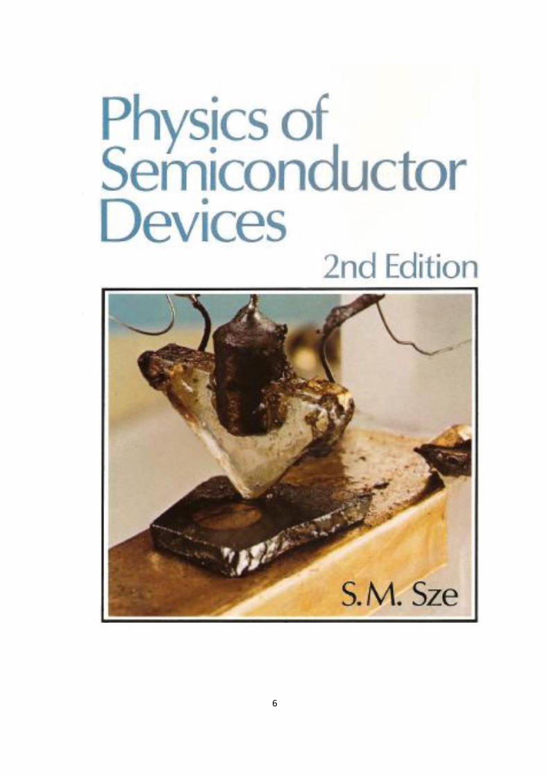
L1 S. M. Sze, Physics of Semiconductor Devices, J. Wiley & Sons, ed. II (15 tiraje), 1982.
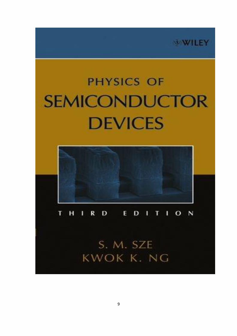
L2 S. M. Sze, Kwok K. Ng, Physics of Semiconductor Devices, Wiley-Interscience, Third Edition,
2007.
L3 E. H. Nicollian, J. R. Brews, MOS Physics and Technology, J. Wiley & Sons, (10tiraje), 1984.
L4 E. H. Nicollian, J. R. Brews, MOS Physics and Technology, Willey Classic Library, 2003.
L5 A. Blicher, Field-Effect and Bipolar Power Transistor Physics, Academic Press, 1981.
L6 J.-P. Colinge, Silicon-On-Insulator Technology: Materials to VLSI, Kluwer Academic
Publishers, 1997.
Ultima carte (L6) foloseste date ale modelului ENSERG pentru tranzistorul MOS, elaborat
impreuna cu colegi romani de la Institutul National Politehnic din Grenoble, in cadrul unei burse de
specializare TEMPRA (1994) – vezi pag. 23 s1 24.

3
Dintre celelalte lucrari, cele mai reprezentative sunt L1 si L2, respectiv Sze, ed. a II-a (1981)
si Sze & Ng, ed. a III-a (2007). Cartea lui Sze (cele doua editii) este cea mai referita lucrare din
domeniul ingineriei actuale si a stiintelor aplicate (vezi pag. 9 si10) cu peste 15.000 de citari (ISI).
Lucrarile de dioda Schottky si strapungerea capacitorului MOS au fost incluse in Sze, ed. a II-
a – vezi paginile 6, 7 si 8. Pana la editia a treia (27 de ani) lucrarea a prelucrat peste 150.000 de
articole din domeniu, introducand elemente de noutate dar si rejectand paragrafe care si-au pierdut
utilitatea. Lucrarile mele au fost pastrate in totalitate in editia a treia, vezi pag. 11 si 12, aceasta
perenitate fiind un factor evident de apreciere si vizibilitate.
Strapungerea capacitorului MOS adresandu-se structurii fundamentale constructive a
tranzistorului MOS (cel mai folosit dispozitiv electronic actual) a fost preluata de multe alte carti in
domeniu.. Lucrarea L3 a lui Nicollian & Brews este cartea de capatai a structurii MOS, de aceeasi
anvergura cu L1 si L2, doar ca are un spectru focalizat al dispozitivelor electronice tratate.. Editata in
1984 si numarand pana astazi 10 tiraje tipografice, a ramas nedetronata prin caracterul ei fundamental,
majoritatea cercetarilor care au urmat in domeniu urmarind in special latura tehnologica a reducerii
dimensiunilor. Ca urmare, in 2003 s-a reeditat, cu acelasi continut in Editura Willey Classic Library
(pag.14). Lucrarile L3 si L4 ale lui Nicollian & Brews preiau strapungerea capacitorului MOS in
doua locuri, insumand 2 pagini (vezi pag. 15 si 16).
Strapungerea capacitorului MOS a rezolvat complet si strapungerea jonctiunii pn, procedura
utila in special pentru dispozitivele de putere. In acest sens lucrarea L5 a lui Blicher preia in afara de
curbele aferente strapungerii capacitorului MOS si modelul fizico-matematic al strapungerii jonctiuni
pn cu poarta, ocupand 5 pagini din carte (vezi pag. 17 … 22).
III. Rabdarea timpului
In acest paragraf voi prezenta traseul unei alte lucrari fundamentale. Pe scurt, aceasta va fi numita
colapsul tensiunii de strapungere.
Istoria incepe cu anul 1967 cand un grup de cercetatori de la Fairchild in frunte cu A. S.
Grove, cunoscut acum ca fondator si presedinte de onoare al INTEL, a publicat un studiu privind
controlul tensiunii de strapungere a jonctiunii pn prin intermediul unui electrod de comanda (poarta)
de tip MOS. Concluziile studiului erau:
C1 – cresterea tensiunii de strapungere a jonctiunii pn odata cu cresterea tensiunii pe poarta cu
o panta aproape unitara;
C2 – limitarea tensiunii de strapungere a jonctiunii pn la o valoare legata de aparitia canalului
sub electrodul de comanda;
C3 – existenta unei caderi puternice a tensiunii de strapungere a jonctiunii pn (colaps) este
sesizata, dar este considerata ca intamplatoare, rezultat al unei tehnologii nepusa la punct.
4
Aceste concluzii au fost intarite de includerea lor in cartea A. S. Grove, Physics and
Technology of Semiconductor Devices, lucrare remarcabila a deceniilor `70 si `80 (tradusa si in
Romania).
Echipa de cercetatori Rusu & Bulucea neaga ultimele doua concluzii: limitarea tensiunii de
strapungere a jonctiunii pn se datoreaza mutarii strapungerii in zona plana a jonctiunii, iar colapsul
este un fenomen fundamental, nedistructiv, constand in mutarea strapungerii in zona capacitorului
MOS. Aceste observatii au fost prezentate la cel mai renumit congres international si au fost publicate
in reviste de top. Dar nu au fost preluate in lucrarea L1 a lui Sze. Motivul, confirmat chiar de S. M.
Sze cu ocazia vizitei sale in Romania in 1994, a fost lipsa unei confruntari directe intre cele doua
puncte de vedere (tinand cont si de notorietatea lui A. S. Grove).
O intamplare fericita face ca in anul 2004, colegul C. D. Bulucea sa gaseasca in arhiva stiintifica
a firmei National Semiconductor (care a preluat firma la care lucra A. S. Grove in 1967) un document
olograf in care acesta isi recunoaste interpretarile gresite aflate in discutie. Aceasta probitate stiintifica
care intareste si mai mult valoarea omului de stiinta A. S. Grove a dat drum liber includerii
fenomenului de colaps in carti de referinta. De aceea, editia din 2007 a lucrarii lui Sze si Ng rezerva
1,5 pagini problemei controlului tensiunii de strapungere a jonctiunii pn cu electrod de poarta, cupland
lucrarea lui Grove care descrie variatia liniara, cu lucrarile romanesti privind colapsul tensiunii de
strapungere. Vezi pag. 13 si indicarea unei referinte cuplate [22] si [23].
Iata o lucrare care a asteptat 27 de ani pentru a fi recunoscuta la cel mai larg si inalt nivel ! In
perspectiva acestei situatii, observatia lui Blicher din 1981, in lucrarea L5, de a pune lucrarile celor doi
competitori impreuna (vezi la pag. 22, 23 si referintele 2.a si 2.b) a fost de natura vizionara. Fara sa fi
transat disputa stiintifica, Blicher a preluat partile pozitive ale celor doi.
Recunoasterea fenomenului de colaps a declansat interesul meu ingineresc pentru o cercetare
aplicativa. Ca urmare, s-a obtinut un contract de la CNCSIS in programul IDEI si s-a declansat o
directie noua de cercetare pentru o noua categorie de circuite electronice bazate pe acest fenomen.
IV. Unele reflectii
Realizarile prezentate pana aici au, fara discutie, o larga vizibilitate internationala. O
caracteristica a vremurilor actuale este incercarea de a trece si la indicatori cantitativi. Nu cunosc insa
vreo modalitate in aceasta situatie. Foile de autoevaluare ARACIS nu prevad acest mod de obtinere a
recunoasterii.
Daca as numara paginile ocupate de realizari proprii in lucrarile L1 … L6 acest indicator este
de 16. In privinta citarilor, unele lucrari sunt orientate spre sursa originala (revista) de aparitie. In
alte situatii, sunt citate global prin cartile de referinta. Lucrarile mele din aceasta categorie fac
parte din cunostintele primare si anume strapungerea dispozitivelor electronice. Daca in aceasta

5
zona se scriu 15 % din articolele stiintifice si brevete, as putea considera ca 15% din numarul total
de citari (15.000, vezi pag. 10), adica 2.250 ma privesc indirect.
Personal, nu-mi doresc aceste cifre. Sunt incantat de aprecierea calitativa a acestor lucrari la
nivelul Academiei Romane.
COPII DUPA CARTILE UNDE SUNT CITATE LUCRARILE FUNDAMENTALE
ALE LUI A. RUSU
6

7
The metal-overlap laterally diffused structure65
is basically a double (parallel)
Schottky diode that does not involve a p-n junction, Fig. 38i. This structure gives nearly
ideal forward and reverse I - V characteristics with very short reverse recovery time.
However, the process involves extra oxidation and diffusion steps, and the outer n - ring
may increase the device capacitance.
[65] A. Rusu. C. Bulucea. and C.Postolache. "The Metal-Overlap-Laterally·Diffused
(MOLD) Schottky Diode.", Solid State Electron.20. 499 (1977).

8
Fig. 31. Breakdown voltage of MIS diode in deep-depletion condition versus silicon doping
concentration with oxide thickness as the parameter. The insert shows the electric field variation along
the Si surface . (After Rusu and Bulucea, Ref. 46.)
The avalanche breakdown in the MOS diode under the deep depletion condition
has been calculated46
based on a two-dimensional model (see Fig. 31, insert). The
electric field along the Si-SiO2, interface shows a peak value Em near the edge of the
gate electrode. The breakdown voltage is defined as the gate voltage that makes the
ionization integral equal to unity when integrated along the line from Em, to a point at
the depletion-layer boundary. Figure 31 shows the result for various oxide thicknesses
and doping concentration s. As can be seen. for a given oxide thickness. a doping exists
which yields minimum breakdown voltage; edge breakdown (i.e., Em> Ei shown in the
insert) dominates to the left of the minimum, and uniform breakdown (i.e Em = Ei )
dominates to the right. Under the uniform breakdown condition, the surface breakdown
field Ei in Si increases with doping (Chapter 2). Therefore, the oxide field E1εs/εi will
increase, resulting in higher voltages. To avoid edge breakdown, the ratio of d/Wmax
must be larger than 0.3 where Wmax is the maximum depletion-layer width at
breakdown.
[46] A. Rusu and C Bulucea, "Deep-Depletion Breakdown Voltage of SiO2/Si MOS
Capacitors", IEEE Trans. Electron Devices, ED-26, 201 (1979)
9

10
Physics of
Semiconductor Devices
Third Edition
S. M. Sze Department of Electronics Engineering
National Chiao Tung University
Hsinchu, Taiwan
and
Kwok K. Ng Central Laboratory
MVC (a subsidiary of ProMOS Technologies, Taiwan)
San Jose, California
With the intention of meeting such a need, the First Edition and the Second Edition of Physics
of Semiconductor Devices were published in 1969 and 1981, respectively. It is perhaps
somewhat surprising that the book has so long held its place as one of the main textbooks for
advanced undergraduate and graduate students in applied physics, electrical and electronics
engineering, and materials science. Because the book includes much useful information on
material parameters and device physics, it is also a major reference for engineers and
scientists in semiconductor device research and development. To date, the book is one of the
most, if not the most, cited works in contemporary engineering and applied science with over
15,000 citations (ISI, Thomson Scientific).

11
The metal-overlap laterally diffused structure77
is basically a double-Schottky diode
(in parallel) that does not involve a p-n junction, Fig. 34i. This structure gives
nearly ideal forward and reverse I-V characteristics with very short reverse
recovery time. However, the process involves extra oxidation and diffusion steps,
and the outer n-ring may increase the device capacitance.
[77] A. Rusu, C. Bulucea, and C. Postolache, “The Metal-Overlap-Laterally-Diffused (MOLD) Schottky
Diode,” Solid-State Electron., 20,499 (1977).

12
Fig. 27 Breakdown voltage of MOS capacitor in deep-depletion condition vs. silicon doping
concentration, with oxide thickness as the parameter. Edge effect causing lower breakdown
has been included. (After Ref. 38.)
The avalanche breakdown voltage in the MOS capacitor under the deep-depletion
condition has been calculated based on a two-dimensional model38
.The results are
shown in Fig. 27 for different doping levels and oxide thickness. It is interesting
to compare these breakdown voltages to those of p-n junctions in Fig. 16a of
Chapter 2. Bear in mind that for similar fields within the semiconductor, an MOS
structure takes a higher bias because of the additional voltage taken up in the
oxide layer. Several interesting features in Fig. 27 should be pointed out. First,
the breakdown voltage VBD, as a function of doping level, has a valley before it
goes up again. The decrease of VBD is the same trend as in a p-n junction due to
the increased field with doping. The rise after the minimum is because at high
doping levels, the higher field at the semiconductor surface at breakdown induces
a larger voltage across the oxide layer, leading to a higher terminal voltage.
Another point is that for lower impurity concentrations, the MOS breakdown is
actually smaller than those of p-n junctions. This is due to the inclusion of the
edge effect in this study. Near the perimeter of the gate electrode, the field is
higher due to the two-dimensional effect which leads to a lower breakdown
voltage.
[38] A. Rusu and C. Bulucea, “Deep-Depletion Breakdown Voltage of SiO,/Si MOS Capacitors,”
IEEE Trans. Electron Dev., ED-26, 201 (1979).

13
Fig. 22 Gate-voltage dependence of breakdown in a gated diode. The location of high-field breakdown shifts with gate bias.
(After Ref. 22.)
Another edge effect that causes premature breakdown is due to an MOS (metal
oxide semiconductor) structure over the junction at the surface. Such a
configuration is often called a gated diode. At certain gate biases, the field near
the gate edge is higher than in the planar portion of the junction and breakdown
changes location from the surface area of the metallurgical junction to the edge of
the gate. This gate voltage dependence of breakdown is shown in Fig. 22. At high
positive gate bias on a p+-n junction, the p
+-surface is depleted while the n-
surface is accumulated. Breakdown occurs near the metallurgical junction at the
surface. As the gate bias is swept more negatively, the location of breakdown
moves toward the n-side (to the right). In the middle gate-bias range, the
breakdown voltage has a linear dependence on the gate bias, with 23
constantmVV GBD (111)
and m≤1. At some high negative gate bias, the field directly under the gate edge
is high enough to cause breakdown, and the breakdown voltage collapses. This
gated diode breakdown phenomenon is reversible and the measurement can be
repeated. To minimize this edge effect, the oxide thickness should be above a
critical value.22
This mechanism is also responsible for the gate-induced drain
leakage (GIDL) of the MOSFET (see Section 6.4.5).
[22] A. Rusu, 0. Pietrareanu, and C. Bulucea, “Reversible Breakdown Voltage Collapse in Silicon Gate-Controlled Diodes,”
Solid-state Electron., 23,473 (1 980).
[23] A. S. Grove, 0. Leistiko, Jr., and W. W. Hooper, “Effect of Surface Fields on the Breakdown Voltage of Planar Siliconp-
n Junctions,” IEEE Trans. Electron Devices, ED-14, 157 (1967).

14
15
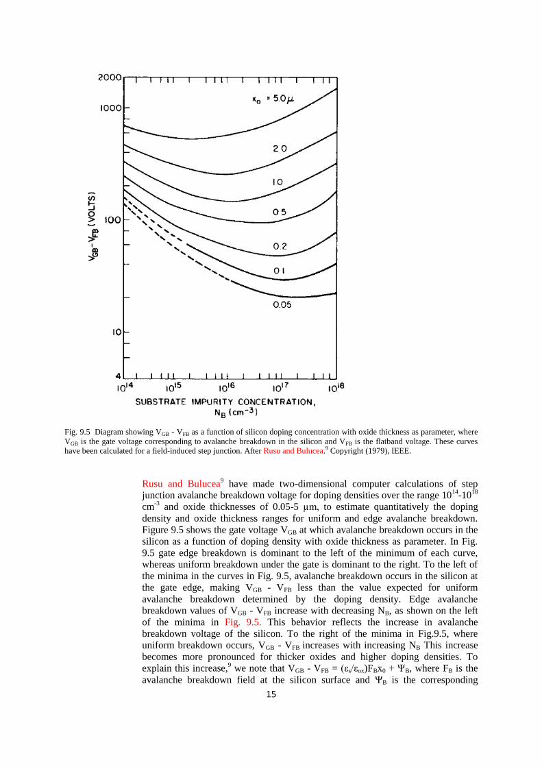
Fig. 9.5 Diagram showing VGB - VFB as a function of silicon doping concentration with oxide thickness as parameter, where
VGB is the gate voltage corresponding to avalanche breakdown in the silicon and VFB is the flatband voltage. These curves
have been calculated for a field-induced step junction. After Rusu and Bulucea.9 Copyright (1979), IEEE.
Rusu and Bulucea9 have made two-dimensional computer calculations of step
junction avalanche breakdown voltage for doping densities over the range 1014
-1018
cm-3
and oxide thicknesses of 0.05-5 µm, to estimate quantitatively the doping
density and oxide thickness ranges for uniform and edge avalanche breakdown.
Figure 9.5 shows the gate voltage VGB at which avalanche breakdown occurs in the
silicon as a function of doping density with oxide thickness as parameter. In Fig.
9.5 gate edge breakdown is dominant to the left of the minimum of each curve,
whereas uniform breakdown under the gate is dominant to the right. To the left of
the minima in the curves in Fig. 9.5, avalanche breakdown occurs in the silicon at
the gate edge, making VGB - VFB less than the value expected for uniform
avalanche breakdown determined by the doping density. Edge avalanche
breakdown values of VGB - VFB increase with decreasing NB, as shown on the left
of the minima in Fig. 9.5. This behavior reflects the increase in avalanche
breakdown voltage of the silicon. To the right of the minima in Fig.9.5, where
uniform breakdown occurs, VGB - VFB increases with increasing NB This increase
becomes more pronounced for thicker oxides and higher doping densities. To
explain this increase,9 we note that VGB - VFB = (εs/εox)FBx0 + ΨB, where FB is the
avalanche breakdown field at the silicon surface and ΨB is the corresponding
16
silicon band bending. For thick oxides and high doping densities, (εs/εox)FBx0 >>
ΨB so that VGB - VFB ≈ (εs/εox)FBx0. The field FB increases with increasing doping
density7,10
causing VGB - VFB to increase with NB in this x0 and NB range.
Breakdown over the entire gate area is necessary to the analysis of avalanche
breakdown experiments. Edge breakdown should be avoided. Edge breakdown
depends on the relative sizes of the oxide and depletion layers as discussed in
Section 9.3.2. Figure 9.5 shows the lowest doping density for which edge
breakdown can be avoided for a given oxide thickness.
Breakdown over the entire area is necessary to the analysis of avalanche
breakdown experiments. Edge breakdown should be avoided. Edge breakdown
depends on the relative sizes of the oxide and depletion layers as discussed in
Section 9.3.2. Figure 9.5 shows the lowest doping density for which edge
breakdown can be avoided for a given oxide thickness.
[9] A. Rusu and C. Bulucea, IEEE Transact. Electron Devices, ED-26, 201 (1979).
17

18
4.1.1 FIELD PLATE OPTIMIZATION
A sufficiently thick field plate oxide prevents inversion and permits
depletion of the n-region under the field plate (Fig. 2). If the oxide is too thick,
however, the n-region will not be depleted enough, however. At the point where
the field plate terminates, i.e., at the plate's edge, the field is highly concentrated
(Fig. 2).
In order to take into account the edge effect [2] in the breakdown
computation, it is necessary to solve a set of two-dimensional Laplace and
Poisson equations for the oxide-field plate system. The Laplace equation applies
to the SiO2 layer, assumed to be charge free. i.e.,
(1)
In silicon the Poisson equation for the fully depleted region is given by
, (2)
where CB is the substrate concentration and εs is the silicon permittivity. Along
the field plate's AB line (Fig. 3a,b [2]), the potential V =VG'=VG-VFB, where VG
is the field plate voltage and VFB is the flat-band voltage. Along the BD line,
0, and along the DFGH line, considered to be in the neutral region, V
= 0. The boundary condition at the HI line in silicon is
, where x0 is the oxide thickness and xd is the
junction depletion region thickness; is the surface potential in the central
planar portion of the device and is equal to , where εs is the
permittivity of silicon. At the IA line in the silicon dioxide, the boundary
condition is
(3)
The computer solution of this set of equations permitted the calculation of
the electric field and potential distributions, which, in turn, allowed the
calculation of the ionization integral and the avalanche breakdown. The MN
field line of the maximum ionization integral was defined as starting at the
maximum field point M, determined for each pair of CB and x0, values and
following the direction of the electric field. The results of the numerical
calculations, plotted in Fig. 4. show that at small oxide thicknesses below 0.1

19
µm and substrate concentrations of less than 1017
cm-3
. The avalanche breakdown
takes place beneath the edge of the metal plate at B' (Fig. 3 [2]) and that the
Fig. 3. Two-dimensional model for the field plate calculations. (a) Metal overlapped planar diode (b)
Region of interest and space-charge field shown at left. Electric field at the interface shown at the bottom. (From
Rusu and Bulucea [2].)
breakdown voltage increases as the substrate concentration decreases. The oxide
voltage drop is small for this range and voltage breakdown takes place in the
field-induced space-charge region in silicon and behaves like the conventional
p-n junction breakdown. However, it is smaller than that of the plane junction
because of the field concentration at the field plate edge.
At large oxide thicknesses, i.e., x0 ≥ 1 µm and CB=1016
cm-3
the
breakdown voltage occurs at the central plane portion of the device, and it
increases as the substrate concentration goes from about 1016
up to 1018
cm-3
.
This is attributed to the field concentrating in the oxide rather than in silicon.
For this range of x0 and CB the voltage drop in the semiconductor is negligibly
small compared to the oxide voltage drop Vox. If the critical field for the
semiconductor breakdown is Ecrit, then the field in the oxide Eoxb at silicon
breakdown is given by
. (4)

20
Fig. 4. Breakdown voltage versus substrate impurity concentration with SiO2 thickness
as a parameter. (From Rusu and Bulucea [2])
The oxide voltage drop at silicon breakdown is therefore
(5)
where BV' = BV - VFB. Since the voltage drop in silicon is negligibly small
BV' VoxbEcrit increases with the background doping, for example. Ecrit 1.5 x
105
V cm-1
at CB=1014
cm-3
. but equals 6 x 10⁵
V cm-1
at CB = 1017
cm-3
. As a
result. the breakdown voltage BV' increases rather unexpectedly with the
background concentration. Equation (5) also shows that BV' varies linearly with
the oxide thickness for the xo and CB range where the approximation of the
negligibly small depletion region drop is valid [2]. i.e.. for CB >> 1016
.
The curves of Fig. 4 show that for a given oxide thickness there is a
substrate concentration that gives a minimum breakdown voltage. To the left of
the minima the edge breakdown dominates: to the right the break- breakdown
due to the plane (central) portion of the depletion region prevails. The electric
field stays uniform at any substrate doping if the condition xo/xdmaxp≥0.3 is
satisfied: xdmaxp is the maximum depletion layer width of the plane junction. The
computer-generated results of Rusu and Bulucea [2] agree reasonably well with
the results of O'Neil and Alonas [1], who came up with a closed form analytical

21
expression for the breakdown voltage of a planar junction provided with a field
plate. The work of [1] also showed that making the oxide thicker reduced the
field crowding effect at the field plate edge and raised the breakdown voltage
similarly to the increase in junction depth. The increase of the oxide thickness
has a greater effect on the field reduction in the silicon substrate than an equal
increment in the junction depth xj. The improvement can be expressed as
(6)
From Eqs. (3.12) and (3.20) we obtain for the cylindrical planar junction
breakdown
, (7)
where xd being the depletion width for a one-sided abrup junction with
the breakdown voltage BVplane. In view of (6), the breakdown voltage is given by
the same expression as (7), but with replaced by
(8)
The analytical expression for the planar junction breakdown voltage with a field
plate is therefore given by
(9)
This relationship is valid for QSS/q values much below 1012
cm-2
(for good
oxides Qss/q is about 1010
cm-2
). An excessively high positive surface charge
increases the breakdown voltage of the n+ -p junction, but degrades the
breakdown of the p+-n junction. Figure 5 represents a plot of this expression for
the breakdown of a planar junction provided with a field plate versus oxide
thickness with CB = ND = 1.1 x 10¹⁴
cm-3
. Also plotted are the experimental data
obtained for planar junctions with radii xj = 4 µm and xj = 9 µm. The agreement
is very good. The formula is applicable to the IC junctions by just changing the
concentration ND to NA for the p-type substrate. An example. breakdown voltage
obtained by [1] for Nd= 1.1 x 10¹⁴
cm-3
with x0 = 10 µm is about 370 V. About
the same breakdown can be obtained from the plot of Fig. 5 [2] for the same
parameters and with VFB -5.0 V.
According to Grove et al. [2a] the breakdown voltage of a p-n junction
depends linearly on the field-plate voltage VG as .
with m 1. However, as VG is increased (more negative for p+-n junctions), a
point is reached when the breakdown voltage suddenly collapses. A small

22
Fig. 5. Planar junction avalanche breakdown voltage as a function of SiO2 oxide
thickness x0. (From O'Neil and Alonas [1].)
change in VG results in a drastic change of the breakdown voltage from a
few hundred volts, for example, to a few tens of volts. The origin of this
effect was attributed by Grove et al. [2a] to the breakdown of the field-
plate-induced junction (inversion). The recent study of Rusu et al. [2b]
explains the collapse as a result of a spatial switching of the avalanche
breakdown within the device structure. It may take place even in the defect-
free crystal. The understanding of the breakdown collapse mechanism makes
Rusu et al. believe that it is possible to extend the diode breakdown up to the
plane junction breakdown without incurring the breakdown fall-down. To
achieve this, the oxide under the field plate should be made thicker than some
minimum value determined by the substrate concentration CB. For example xob
at CB = 2 x 10¹⁴
cm-3
equals ~ 10 µm: at CB = 1015
cm-3
, it equals 2.2 µm. At CB
= 1016
cm-3
, the critical thickness drops down to only 0.2 µm.
It should be pointed out that the field-plate-controlled p+-n diodes, which had
been previously avalanched at high reverse voltages, show higher breakdowns
due to the injection of positive charges (holes) into the oxide. Positive oxide
charging appears to be equivalent in silicon to an increase in the oxide thickness.
2. A. Rusu and C. Bulucea , IEEE Trans. Electron Devices ED-26, 201 (1979).
2a. A.S. Grove, O. Leistiko, Jr., and W.W. Hooper, IEEE Trans. Electron Devices ED-14,
157 (1967).
2b. A. Rusu, O. Pietrareanu, and C. Bulucea, Solid-State Electronics, 23, 473
23
SILICON-ON-INSULATOR
TECHNOLOGY:
Materials to VLSI
2nd Edition
by
Jean-Pierre Colinge
Universite catholique de Louvain, Belgium
KLUWER ACADEMIC PUBLISHERS
Boston I Dordrecht I London
24
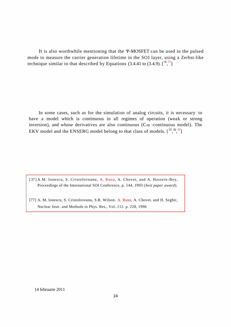
It is also worthwhile mentioning that the Ψ-MOSFET can be used in the pulsed
mode to measure the carrier generation lifetime in the SOI layer, using a Zerbst-like
technique similar to that described by Equations (3.4.41 to (3.4.9). [76
,77
]
In some cases, such as for the simulation of analog circuits, it is necessary. to
have a model which is continuous in all regimes of operation (weak or strong
inversion), and whose derivatives are also continuous (C -continuous model). The
EKV model and the ENSERG model belong to that class of models. [35
,36
,37
]
14 februarie 2011
[ 3 7 ] A.M. Ionescu, S. Cristoloveanu, A. Rusu, A. Chovet , and A. Hassein -Bey,
Proceedings of the International SOI Conference, p. 144, 1993 (best paper award).
[77] A. M. Ionescu, S. Cristoloveanu, S.R. Wilson. A. Rusu, A. Chovet. and H. Seghir,
Nuclear Instr. and Methods in Phys. Res., Vol..112. p. 228, 1996